introduction
With the continuous development of new technologies, digital substations are emerging. Driven by smart grid planning, digital substations will become the mainstream of new substations in the future. As we all know, the number of power grid signals is extremely large and highly correlated, which brings great troubles to collection, calculation and real-time monitoring. In order to solve this problem. The designer of this article built an intelligent IED (Intelligent Electronic Device, intelligent power monitoring device) based on DSP and CPLD, which can collect multiple signals at the same time and obtain key data of power grid operation through FFT algorithm.
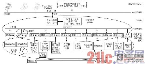
The logic of the smart substation based on IEC61850 is shown in Figure 1. The IEC61850 protocol mainly defines the information hierarchical structure of the substation: process layer, station control layer and bay layer. This paper focuses on the study of smart IED devices. According to the description of the IEC61850 protocol, the IED detection equipment is located in the bay layer and process layer. Among them, the main IED responsible for storing measurement data, performing grid data analysis and diagnosis is located in the bay layer; the measurement IED that is directly connected to the field sensor is located in the process layer; the existing computer system of the substation at the station control layer will store long-term historical data and diagnostic results.

Figure 1 Logic block diagram of smart substation
1 System Hardware Design
The system consists of an algorithm module built with DSP, CPLD and high-speed A/D converter, a multi-channel selection data acquisition module and a signal filtering module. The DSP is responsible for data acquisition, which is currently a more mainstream industrial control DSP. The CPLD uses Altera's EPM3256, and the A/D converter uses Maxim's 14-bit high-speed chip MAX125. The DSP focuses on the calculation of power grid energy quality, while the circuit constructed by CPLD and high-speed A/D converter is suitable for the simultaneous acquisition of multiple signals.
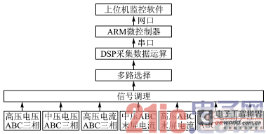
The processing flow of the intelligent IED is shown in Figure 2. The detected signals are mainly three-phase voltage and three-phase current signals. The signal front-end circuit will perform a low-pass filtering function to filter out the clutter that has a greater impact on the signal. The signal is then collected by a high-speed A/D converter, implemented through an A/D converter + CPLD circuit, and finally sent to the DSP through the data bus. After completing the parameter calculation, the DSP packages the data format in a unified manner and uploads it to the master control IED. Its main function is to receive the data of the detected IED and upload it to the database.

Figure 2 Intelligent IED processing flow
1.1 Multi-way selector switch
This system collects many objects. Since the calculation of power factor angle and dielectric loss angle must be the phase difference between voltage and current at the same time, the three-phase current value and the three-phase end-screen current value corresponding to the three-phase voltage must be collected at the same time. MAX125 is a dual-channel 8-way collection, each of which can collect 4 signals. In this system, 3 of them will be used, and the other signal can be idle.
1.2 Communication interface with host computer
In fact, this system is just a data acquisition module of the entire intelligent transformer. All collected signals need to be packaged and transmitted to the host computer after processing. This system adopts a simple RS232 transmission method. All data is transmitted to the host computer at one time, and then packaged by the host computer and transmitted to the monitoring center through TCP/IP.
1.3 Data acquisition and A/D conversion module
Smart grids need to collect at least 20 signals, including high and low three-phase voltage, three-phase current, three-phase end-screen current and neutral point current. These signals are converted into voltage signals through sensors and input into the monitoring device.
This system requires the calculation of harmonic content above 13 times, and the FFT algorithm collects at least 128 points in 2 power grid cycles. The power grid frequency is 50 Hz, which means that 128 working points must be collected in 40 ms, and the collection frequency is 3200 Hz. In order to ensure that the collected points are concentrated in two complete cycles, it is necessary to use DSP timing interrupt to collect working points. In the whole system, the conversion accuracy of the signal acquisition unit plays a vital role in the performance of the whole system. MAX125 has its own sample and hold, and the channels are sampled simultaneously with a sampling accuracy of 14 bits, which is suitable for the simultaneous sampling of voltage and current of the power grid at a certain moment; the input voltage range is ±5 V, and the time to collect one channel is 3 μs, which is very suitable for high-speed acquisition systems.
When MAX125 completes the conversion of the sampled 8-channel signal, its INT pin generates an interrupt signal, which is connected to the custom INT pin in the CPLD to indicate that the conversion is complete. The DSP can read and process the sampled signal by responding to the interrupt. MAX125 selects the channel by programming the address lines A0~A3. The CLK signal is used as the clock required for A/D conversion and is provided by the clock of the CPLD. The data bus (D0~D13), clock input CLK, chip select input CS, write input WR, read input RD, conversion start input CONVST and interrupt output INT pin of MAX125 are all connected to the corresponding function I/O pins defined in the CPLD. Since this system needs to synchronously collect 20 front-end signals, and MAX125 is an 8-channel differential input A/D conversion chip, this system requires 3 MAX125 chips.
1.4 Signal Conditioning Circuit
The signal from the transformer of 220 kV or above has to pass through the complex environment on site before entering the sensor. The signal from the sensor to MAX125 has to be transmitted through a long line. Its signal usually cannot be directly received by the control unit, so the signal conditioning circuit becomes an indispensable part of the control system. Generally speaking, the 20 mA standard current signal is converted into a 1~5 V standard voltage signal at the differential input end, and then input into the A/D converter after conditioning by the signal conditioning circuit. The output voltage is higher than the input voltage value of the A/D converter, and sampling is performed after voltage division.
A large number of nonlinear loads in the power system will greatly reduce the power quality of the power grid. If the signals collected from the power grid are not processed, the calculation accuracy of the DSP will be affected. The signal processing in this system uses a low-pass filter. The low-pass filter module generally uses circuit elements (such as resistors, capacitors, and inductors) to form the required frequency characteristic circuit. An ideal low-pass filter can completely eliminate all frequency signals above the cutoff frequency, and signals below the cutoff frequency can pass unaffected.
2 System Software Design
2.1 Software Process
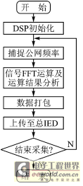
First, the corresponding functions of the DSP are initialized, including the serial port, timer interrupt, and some I/O ports used as control lines. Before data processing, an EVA module must be turned on to capture the frequency of the power grid. The subsequent work is to read the data from the A/D converter, a group of 128 corresponding to the voltage, current and end-screen current values of two cycles. FFT calculation is performed on each 128 data, and the calculation results will be further analyzed to obtain the power factor, dielectric loss angle and other values. The process of IED data collection, calculation, and upload is shown in Figure 3.

Figure 3 IED data collection, calculation, and upload process
The parameters that need to be calculated by DSP are the effective values of the three-phase voltage and current of high voltage A, B, and C, the effective values of the three-phase voltage and current of medium voltage A, B, and C, the amplitude and harmonic distortion rate of the 2-13 harmonics of each phase voltage and current, and the power factor and dielectric loss angle of the three phases of high and medium voltage. The problem that the DSP algorithm needs to solve is to calculate the 2-13 harmonics and the power factor of each phase. The core of the algorithm is the FFT algorithm.
Smart grids need to collect at least 20 signals. First, the relevant functions of the DSP are initialized, including the serial port, GPIO, EVA event capture module and timer interrupt. Then, the common I/O pins are used as trigger signals to select multiple A/D input signals in turn. These signals can be sampled through the MAX125 after the signal waveform is stable through the signal conditioning circuit. The data is transmitted to the DSP through the data bus. After a series of operations, the DSP obtains the power factor, dielectric loss fundamental harmonic content, and packages these data in a certain data format and sends them to the ARM microcontroller through the serial port. ARM then transmits these data to the host computer monitoring software.
The specific code is as follows:
void GETDATA1_A128(){
int k;
GpioDataRegs.GPBSET.all=0xFFFF; //Set all GPIOBs to 1
asm(""RPT #1 || NOP""); //Send a negative pulse first
GpioDataRegs.GPBCLEAR.bit.GPIOB10=1;
GpioDataRegs.GPBSET.bit.GPIOB6=1; //Control write instruction
GpioDataRegs.GPBSET.bit.GPIOB0=1; //Select channel A, convert all 4 channels together
GpioDataRegs.GPBSET.bit.GPIOB1=1; //Write 0011
GpioDataRegs.GPBCLEAR.bit.GPIOB2=1;
GpioDataRegs.GPBCLEAR.bit.GPIOB3=1;
GpioDataRegs.GPBCLEAR.bit.GPIOB4=1; //WR write negative pulse signal
asm(""RPT #4 || NOP"");//30 ns
GpioDataRegs.GPBSET.bit.GPIOB4=1;
GpioDataRegs.GPBSET.bit.GPIOB10=1; //CS chip select pulse signal
asm(""RPT #1 || NOP"");//延时30 ns
GpioDataRegs.GPBCLEAR.bit.GPIOB12=1; //RD signal is pulled low
asm(""RPT #12 || NOP""); //After the rising edge of CS, delay 125 ns
for(i=0;i<128;i++) {
GpioDataRegs.GPBCLEAR.bit.GPIOB5=1; //Conversion trigger signal
asm(""RPT #4 || NOP"");//延时30 ns
GpioDataRegs.GPBSET.bit.GPIOB5=1; //Conversion trigger signal
for(k=0;k<555;k++){//Delay 12 μs, wait for conversion to complete
asm(""RPT #1 || NOP"");
}
……
}
}
2.2 Calculation of power grid parameters
After receiving the A/D converted data, DSP will immediately start calculation. In this design, the harmonic content and harmonic factors of the power grid are a key point of calculation. The fundamental reason for the generation of harmonics in the power system is due to nonlinear loads. When the current flows through the load, it is not linearly related to the applied voltage, forming a non-sinusoidal current, that is, harmonics are generated in the circuit. The harmonic frequency is an integer multiple of the fundamental frequency. According to the Fourier analysis principle, any repetitive waveform can be decomposed into a sine wave component containing the fundamental frequency and a series of harmonics that are multiples of the fundamental frequency. Harmonics are sine waves, and each harmonic has a different frequency, amplitude and phase angle.
Harmonics can be divided into even and odd harmonics. Generally speaking, odd harmonics cause more and greater harm than even harmonics. In a balanced three-phase system, due to the symmetry relationship, even harmonics have been eliminated, and only odd harmonics exist. The FFT algorithm can be used to decompose the grid voltage/current into a superposition of 50 Hz fundamental wave and multiple harmonics. In this way, the harmonics in a specific frequency band are obvious.
In addition to the calculation of harmonics, which requires the use of FFT algorithms, the system also has other parameter calculations. Since the function modules called are very complex, only the calculation process of some parameters is described. Most parameters are obtained through discrete integration of the acquisition points.
High voltage A phase voltage effective value:
High voltage A phase current effective value:
Single-phase voltage/current harmonic distortion rate:
Medium voltage A phase current harmonic content:
Total harmonic distortion rate of high-voltage three-phase voltage: calculate the harmonic content and fundamental content of each phase voltage, and divide the total harmonic content by the fundamental component.
Single-phase voltage power factor: The arc tangent value of the (imaginary part/real part) of the fundamental effective value obtained by the FFT algorithm.
Single-phase dielectric loss: Perform FFT operations on the end-screen current and the corresponding phase voltage respectively, and make the difference in the obtained phases. The phase difference angle is the dielectric loss angle.
3 Conclusion
The system is applied to the intelligent transformer system, which can collect multiple channels synchronously with high conversion accuracy. The experiment proves that the real-time and accuracy of the signal acquisition module have achieved good results, and the operation is stable and reliable. The system adopts a high-speed 14-bit parallel A/D converter, which simplifies the interface design and improves the reading speed and data processing speed. Various complex control signals are realized through CPLD, and the external SRAM and Flash can be mapped to the data space or program space by changing the level of the XF pin. The DSP chip is connected to the high-precision data acquisition chip MAX125 through the CPLD chip to realize multi-channel high-speed synchronous real-time data acquisition of the signal, with strong anti-interference ability, and the FFT algorithm is used to accurately calculate the harmonic factor, power angle, and dielectric loss angle of the power grid.
Previous article:Design of Interface between DSP and Intelligent Color LCD Display
Next article:Interface control between DSP chip and touch screen
- Popular Resources
- Popular amplifiers
- Red Hat announces definitive agreement to acquire Neural Magic
- 5G network speed is faster than 4G, but the perception is poor! Wu Hequan: 6G standard formulation should focus on user needs
- SEMI report: Global silicon wafer shipments increased by 6% in the third quarter of 2024
- OpenAI calls for a "North American Artificial Intelligence Alliance" to compete with China
- OpenAI is rumored to be launching a new intelligent body that can automatically perform tasks for users
- Arm: Focusing on efficient computing platforms, we work together to build a sustainable future
- AMD to cut 4% of its workforce to gain a stronger position in artificial intelligence chips
- NEC receives new supercomputer orders: Intel CPU + AMD accelerator + Nvidia switch
- RW61X: Wi-Fi 6 tri-band device in a secure i.MX RT MCU
 Professor at Beihang University, dedicated to promoting microcontrollers and embedded systems for over 20 years.
- LED chemical incompatibility test to see which chemicals LEDs can be used with
- Application of ARM9 hardware coprocessor on WinCE embedded motherboard
- What are the key points for selecting rotor flowmeter?
- LM317 high power charger circuit
- A brief analysis of Embest's application and development of embedded medical devices
- Single-phase RC protection circuit
- stm32 PVD programmable voltage monitor
- Introduction and measurement of edge trigger and level trigger of 51 single chip microcomputer
- Improved design of Linux system software shell protection technology
- What to do if the ABB robot protection device stops
- CGD and Qorvo to jointly revolutionize motor control solutions
- CGD and Qorvo to jointly revolutionize motor control solutions
- Keysight Technologies FieldFox handheld analyzer with VDI spread spectrum module to achieve millimeter wave analysis function
- Infineon's PASCO2V15 XENSIV PAS CO2 5V Sensor Now Available at Mouser for Accurate CO2 Level Measurement
- Advanced gameplay, Harting takes your PCB board connection to a new level!
- Advanced gameplay, Harting takes your PCB board connection to a new level!
- A new chapter in Great Wall Motors R&D: solid-state battery technology leads the future
- Naxin Micro provides full-scenario GaN driver IC solutions
- Interpreting Huawei’s new solid-state battery patent, will it challenge CATL in 2030?
- Are pure electric/plug-in hybrid vehicles going crazy? A Chinese company has launched the world's first -40℃ dischargeable hybrid battery that is not afraid of cold
- Differences between MSP430 programmer emulator and JTAG, SBW, and BSL interfaces
- BUCK circuit simulation and experiment
- Is there a dedicated chip for PWM output of I2C interface?
- Registration for the prize live broadcast is open | TOF (Time of Flight) technology introduction and product application
- Zero-knowledge open source sharing-the use of ESP8266WIFI module
- STM32CUBEMX generates EWARM V8 project, but cannot open the project
- System performance indicators of single-phase sine wave inverter
- PADS PCB board partial circuit replication
- Phantom Power in Audio Equipment
- View Circuit-CSA and System

 AD621ARZ


 京公网安备 11010802033920号