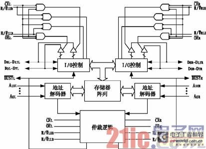
This paper introduces a method of realizing high-speed data communication between DSP and single-chip microcomputer by using dual-port RAM, and gives the interface circuit and software implementation scheme between them. Keywords: DSP; dual-port RAM; interface circuit; data communication 1 Introduction Digital signal processor (DSP) is a microprocessor suitable for implementing various digital signal processing operations. It has the following main structural features: (1) It adopts an improved Harvard structure with independent program bus and data bus, which can access instruction and data space at the same time, allowing actual transmission between program memory and data memory; (2) It supports pipeline processing. The processor divides the operation of each instruction into several stages such as instruction fetch, decoding, and execution. At a certain moment, several instructions are processed at different stages at the same time; (3) The chip contains a dedicated hardware multiplier, so that multiplication can be completed in a single cycle; (4) The special instruction structure and addressing mode meet the requirements of digital signal processing FFT, convolution and other operations; (5) The fast instruction cycle can process tens of millions or even hundreds of millions of fixed-point or floating-point operations per second; (6) Most of them are equipped with a separate DMA bus and its controller, which can perform high-speed parallel data transmission without basically affecting the digital signal processing speed. A complete control system can be formed by a DSP plus memory, analog/digital conversion unit and peripheral interface, but this solution is not feasible to achieve high-speed real-time control. Because a real-time control system generally needs to complete tasks such as data acquisition, analog/digital conversion, analysis and calculation, digital/analog conversion, real-time process control and display, relying on a single DSP to complete these tasks will inevitably greatly extend the system's control cycle for the control object, thereby affecting the performance of the entire system. Therefore, we add a CPU to be responsible for tasks such as data acquisition, analog/digital conversion, process control and human-machine interface, so that the DSP can focus on the implementation of the system control algorithm and make full use of its high-speed data processing capabilities. From the perspective of performance-price ratio, this CPU uses an 8-bit 51 series microcontroller. At this time, data sharing between the two CPUs becomes an important issue. The use of dual-port RAM (DRAM for short) is an effective way to solve the data sharing between CPUs. Compared with serial communication, the use of dual-port RAM not only has a high data transmission speed, but also has good anti-interference performance. In the active power filter developed by the author's laboratory, TI's third-generation DSP chip TMS320C32 and 51 series microcontroller 89C52 were selected as the CPU of the control system. The data exchange between the two CPUs is completed through the dual-port RAM CY7C133. However, in actual use, the problem of mismatch between the bus width of 89C52 and the dual-port RAM is encountered, and the interface circuit needs to be designed. 2 Internal structure and function of dual-port RAM CY7C133 CY7C133 is a high-speed 2K%26;#215;16CMOS dual-port static RAM developed by CYPRESS. It has two sets of independent and completely symmetrical address buses, data buses and control buses. It adopts 68-pin PLCC package and the maximum access time can be 25/35/55 ns. The master-slave mode can easily expand the data bus to 32 bits or wider. The functions of each pin are shown in Table 1, and the internal function block diagram is shown in Figure 1.

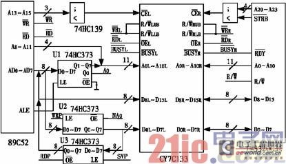
CY7C133 allows two CPUs to read any storage unit at the same time (including reading the same address unit at the same time), but does not allow writing at the same time or reading and writing the same address unit at the same time, otherwise an error will occur. The arbitration logic (busy logic) circuit is introduced in the dual-port RAM to solve this problem: when the left and right ports write or read and write the same address unit at the same time, the first stable address port is given priority to read and write through the arbitration logic circuit, and at the same time the internal circuit makes the signal of the other port valid, and prohibits the other party from accessing it internally until the operation of this port is completed. The BUSY signal can be used as an interrupt source to indicate that this operation is illegal. In the master-slave mode, the signal of the master chip is connected to the pull-up resistor as the output, and the signal of the slave chip is used as the write-inhibit input. 3 Interface circuit between DSP, single-chip microcomputer and dual-port RAM The address bus width of 89C52 is 16 bits and the data bus is 8 bits; the data bus width of TMS320C32 is 32 bits and the address bus width is 24 bits. The data bus width of CY7C133 is 16 bits, and the address bus width is 11 bits, so there is nothing special about the interface between TMS320C32 and dual-port RAM, but the interface circuit between 89C52 and dual-port RAM requires bus expansion of 89C52. The specific method is to use the latch function of latch 74HC373, control its enable signal, perform time-sharing reading and writing, and realize the expansion of data bus, that is, use latch as virtual bus. The specific reading and writing process, the generation of reading and writing signals and latch enable signal will be described in detail below. The interface circuit between DSP, single-chip microcomputer and dual-port RAM is shown in Figure 2.

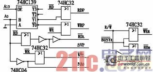
The address space allocated to the dual-port RAM by TMS320C32 is 0x800000h~0x8007FFh. A20~A23 and STRB are decoded by 38 decoder 74HC138 to give the chip select signal CER of the dual-port RAM. The address space allocated to the dual-port RAM by 89C52 is 0x1000h~0x1FFFh. A13~A15 are decoded by 24 decoder 74HC139 to generate the chip select signal CEL of the dual-port RAM. Each side of the dual-port RAM has two read/write control signals, which control the read/write of the high byte and the low byte respectively. When in use, the high and low bits of the data can be written separately as needed. In the interface circuit shown in Figure 2, the two read/write control signals on both sides are connected together, that is, the read and write of the dual-port RAM are both 16-bit data at the same time. The generation of the read and write signals of the dual-port RAM CY7C133 and the enable signal of the latch 74HC373 in Figure 2 is shown in Figure 3. Among them, WR is the write control signal of 89C52, RD is the read control signal of 89C52, A0 is the lowest address bit of 89C52, A15 is the highest address bit, R/W is the read and write control signal of TMS320C32, BUSYL is connected to a pin of the P1 port of 89C52 (the specific selection can be made according to the actual situation of the system, not shown in the figure), and BUSYR is connected to the READY signal of TMS320C32.

The following is a discussion of the reading and writing process of 89C52 to dual-port RAM. When 89C52 reads data from dual-port RAM, it can be seen from Figure 3 that A0 should be low at this time. Assuming that the address is 0x1000h, the 16-bit data stored at this address in the dual-port RAM is read out at the same time. Since the high 8-bit data line is directly connected to the 8-bit data line of 89C52, the high 8-bit data is immediately read into 89C52. At the same time, according to the mutual logical relationship of each signal in Figure 3, it is not difficult to judge that the enable signal LE of U3 is valid (high level) and OE is invalid (low level), so the low 8-bit data is sent to U3 and latched. Then 89C52 performs another read operation. At this time, the address becomes 0x1001h. Since A0 becomes high level, the read enable signal of the dual-port RAM becomes invalid level, so this read operation has no effect on the dual-port RAM. Let's look at the changes of U3's enable signals LE and OE. Obviously, LE becomes an invalid level, while OE becomes a valid level. The data latched last time (i.e., the lower 8-bit data of the dual-port RAM) is sent to 89C52. When 89C52 writes to the dual-port RAM, note that A0 should be high at this time. Assuming the address is 0x100Ch, it can also be judged from Figure 3 that U2's enable signals LE and OE are both valid levels, so the data is written into the dual-port RAM at the same time (i.e., the upper 8-bit data and the lower 8-bit data of the dual-port RAM are the same at this time); then 89C52 performs another write operation, and the address becomes 0x100Dh. Since A0 becomes a low level, U2's chip select is an invalid level, U2 is blocked, and the data is written into the upper 8 bits of the dual-port RAM. From the above analysis, we can know that by using the different levels of the lowest address bit A0, 89C52 successfully realizes the reading or writing of data in the dual-port RAM through two consecutive read or write operations. The only difference is that when reading, the high 8 bits are read first and the low 8 bits are read later; while when writing, the low 8 bits are written first and the high 8 bits are written later. 4 Software Implementation Scheme The dual-port RAM must adopt a certain mechanism to coordinate the reading and writing operations of the left and right CPUs, otherwise there will be errors in reading and writing data. Usually, interrupts, hardware, tokens and software can be used to coordinate the two sides. This article adopts the software method. From the above analysis, we can know that in the interface circuit, the lowest address bit A0 of 89C52 has actually been used to divide the storage space of the dual-port RAM into two spaces of odd and even addresses. Among them, the odd address space is dedicated to 89C52 writing, and the even address space is dedicated to 89C52 reading. Then we only need to make corresponding processing on the software of TMS320C32, that is, TMS320C32 reads only the odd address space of the dual-port RAM and writes only the even address space. This avoids the TMS320C32 and 89C52 writing operations to the same address unit of the dual-port RAM. In addition, before accessing the dual-port RAM, the CPU first queries the BUSY signal of the local end, and only performs read and write operations when the local /BUSY signal is invalid, further ensuring the reliability of data reading and writing. 5 Conclusion The data communication between the dual CPUs is realized through the dual-port RAM, which greatly improves the data transmission speed and reliability, and meets the real-time and high-speed control requirements of the control system. The interface circuit between the 89C52 and the dual-port RAM designed in this paper is simple and practical, successfully solving their bus matching problems, and has certain reference value for other similar systems that require bus expansion.
Previous article:Method of realizing serial communication between high-speed DSP and PC
Next article:Design of local meteorological monitoring system for power transmission lines based on DSP and CPLD
- Popular Resources
- Popular amplifiers
- Huawei's Strategic Department Director Gai Gang: The cumulative installed base of open source Euler operating system exceeds 10 million sets
- Analysis of the application of several common contact parts in high-voltage connectors of new energy vehicles
- Wiring harness durability test and contact voltage drop test method
- Sn-doped CuO nanostructure-based ethanol gas sensor for real-time drunk driving detection in vehicles
- Design considerations for automotive battery wiring harness
- Do you know all the various motors commonly used in automotive electronics?
- What are the functions of the Internet of Vehicles? What are the uses and benefits of the Internet of Vehicles?
- Power Inverter - A critical safety system for electric vehicles
- Analysis of the information security mechanism of AUTOSAR, the automotive embedded software framework
 Professor at Beihang University, dedicated to promoting microcontrollers and embedded systems for over 20 years.
- LED chemical incompatibility test to see which chemicals LEDs can be used with
- Application of ARM9 hardware coprocessor on WinCE embedded motherboard
- What are the key points for selecting rotor flowmeter?
- LM317 high power charger circuit
- A brief analysis of Embest's application and development of embedded medical devices
- Single-phase RC protection circuit
- stm32 PVD programmable voltage monitor
- Introduction and measurement of edge trigger and level trigger of 51 single chip microcomputer
- Improved design of Linux system software shell protection technology
- What to do if the ABB robot protection device stops
- Allegro MicroSystems Introduces Advanced Magnetic and Inductive Position Sensing Solutions at Electronica 2024
- Car key in the left hand, liveness detection radar in the right hand, UWB is imperative for cars!
- After a decade of rapid development, domestic CIS has entered the market
- Aegis Dagger Battery + Thor EM-i Super Hybrid, Geely New Energy has thrown out two "king bombs"
- A brief discussion on functional safety - fault, error, and failure
- In the smart car 2.0 cycle, these core industry chains are facing major opportunities!
- The United States and Japan are developing new batteries. CATL faces challenges? How should China's new energy battery industry respond?
- Murata launches high-precision 6-axis inertial sensor for automobiles
- Ford patents pre-charge alarm to help save costs and respond to emergencies
- New real-time microcontroller system from Texas Instruments enables smarter processing in automotive and industrial applications
- Playing with Circuits (1) - High-Side Current Detection
- 【Live FAQ】OMRON relay, switch and connector solutions for photovoltaic inverters/energy storage systems
- In the era of autonomous vehicles: Antenna measurement and simulation are more critical than ever
- 3 Benefits of Using Low IQ Buck/Boost Converters to Extend Flow Meter Battery Life
- Introduction to Power Factor Correction Technology in AC/DC Front-End Converter Modules
- Raspberry Pi Foundation Launches $4 Raspberry Pi Pico with MicroPython Support
- EEWORLD University ---- Overcurrent Sensing Technology
- [Zero-knowledge ESP8266 tutorial] Quick Start 23 Applying OLED
- SIMterix-Simplies~3~ Verilog-A
- C2000 Power-on Boot Mode Analysis

 LM139W/883B


 京公网安备 11010802033920号