1 Introduction
The rapid development of modern wireless communications is increasingly moving towards increasing information capacity, improving channel spectrum utilization and improving linearity. On the one hand, people widely use high-power microwave transistors working in Class A and B states to improve transmission power and utilization efficiency; on the other hand, the introduction of passive devices and active devices, the adoption of multi-carrier configuration technology, etc., will lead to Intermodulation distortion of signals. Therefore, when designing a radio frequency power amplifier, it must be linearized so that the output signal can obtain better linearity. Commonly used linearization technologies include: power backoff, predistortion, feedforward, etc. Among them, power backoff technology can effectively improve the linearity of narrowband signals, while predistortion technology and feedforward technology, especially feedforward technology, Due to its advantages of high calibration accuracy, high stability and no bandwidth limitation, it has become the main technology used to improve the linearity of broadband signals. This article first briefly describes the common feedforward linearization technology, and then improves it on this basis, adds an adaptive algorithm, and extracts out-of-band signals through signal envelope detection technology for adjustment, thereby improving the linearity of the output signal. Purpose.
2. Basic principles of feedforward
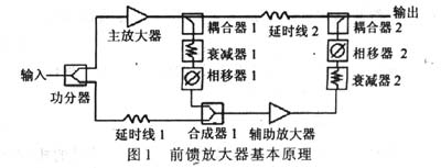
The most basic feedforward amplifier principle is shown in Figure 1. It consists of 2 loops: Loop 1 consists of power divider, main amplifier, coupler 1, attenuator 1, phase shifter 1, delay line 1, and synthesizer 1. The input RF signal, that is, two pure carrier signals, is divided into two branch signals after a power splitter: the upper branch is the main power amplifier branch, and the pure RF carrier signal passes through this branch to generate an amplified carrier wave signal and intermodulation distortion signal; the lower branch is an additional branch. The pure RF carrier signal is delayed after passing through this branch. The nonlinear distortion signal output by the main power amplifier branch passes through attenuator 1 and phase shifter 1. , combined with the signal output from the attached branch in synthesizer 1, adjust attenuator 1 and phase shifter 1 so that the two branch signals obtain equal amplitude, 180' phase difference and equal delay. At this time, the RF carrier signal of the main power amplifier branch can be effectively offset, and the intermodulation distortion signal generated by the nonlinear amplification of the main amplifier can be extracted. Therefore, this loop is also called the RF carrier signal cancellation loop.

Loop 2, also called the distortion signal elimination loop, consists of delay line 2, auxiliary amplifier, attenuator 2, phase shifter 2, and coupler 2. There are also two branches: the upper branch delays the nonlinear distortion signal output by the main amplifier and sends it to the coupler 2; the lower branch amplifies, attenuates, and phase-shifts the intermodulation distortion signal extracted from loop 1. Finally, it is sent to coupler 2, and attenuator 2 and phase shifter 2 are adjusted until the intermodulation distortion signal in the signal output by coupler 2 is the smallest, that is, the IMD is the smallest, then the output signal at this time is an amplified RF signal. .
3. Adaptive feedforward RF power amplifier
3.1 Principle and algorithm of adaptive feedforward circuit
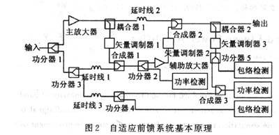
Since the carrier signal cancellation requirements in the feedforward system are very high, changes in the internal and external environments, such as changes in input signal power, DC bias voltage, and ambient temperature, can easily cause the carrier signal cancellation to malfunction. Therefore, it becomes very necessary to introduce adaptive technology to obtain the matching of carrier signal in amplitude, phase and delay in time. The structure of the adaptive feedforward system is shown in Figure 2.

It consists of three loops: loop 1 is mainly used to extract intermodulation distortion signals, loop 2 is mainly used to eliminate distortion signals, and loop 3 is mainly used to detect intermodulation distortion signal power.
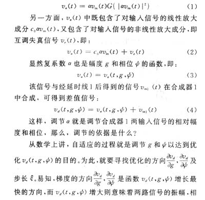
Assume that the input signal is υin(t), and the output signal after passing through the main amplifier is υρα(t). Couple part of υρα(t) to vector modulator 1, and use complex coefficient α to represent the modulation coefficient of vector modulator 1. At the same time, Simplifying the main amplifier into a memoryless nonlinear model, its AM/AM and AM/PM transfer functions can be simply expressed by the complex voltage gain G(χ), where χ represents the instantaneous power, then from the vector synthesizer 1The output signal υα(t) can be expressed as:


In terms of the specific implementation structure, a power divider 2 is added after the synthesizer 1. Its purpose is to detect the power of the signal υd (t, g, ψ). Obviously, if α is adjusted so that the two input signals of the synthesizer 1 The amplitude, phase and delay of The power is small enough, then the adjustment of α is optimal at this time, that is, the RF carrier signal has been eliminated to the greatest extent, and only the intermodulation distortion signal υe(t) remains.
The intermodulation distortion signal entering loop 2 is amplified by the auxiliary amplifier, adjusted by vector modulator 2 (the modulation coefficient is a complex coefficient β), and then combined with the main amplifier output signal passing through delay line 2 in synthesizer 2. This loop also uses adaptive technology to adjust the amplitude and phase of the intermodulation distortion signal. Its mathematical principle is as mentioned above, but its implementation structure is different from loop 1. Loop 1 uses a direct detection synthesizer. The output signal of 1 is used to determine whether the RF carrier signal is offset to a minimum value, while loop 2 needs to introduce a third loop when determining whether the intermodulation distortion signal is offset to a minimum value.
We know that for the same power output signal, the envelope of the linear signal is larger than the envelope of the nonlinear signal, and the envelope difference signal between the two is the intermodulation distortion signal. Minimize the envelope difference signal. This can improve the linearity of the output signal to the greatest extent, thereby reducing IMD. This is how Loop 3 works. One of the two signals he processes is a linear signal, that is, the RF carrier signal that passes through the delay line 3 and the power divider 4, and the other is a nonlinear signal, that is, it is synthesized by the synthesizer 2 after passing through the feedforward system loop 1 and loop 2. output signal. First, the loop detects the power of the combined signal of the two signals and adjusts the vector modulator 3 until the detected power is minimum. At this time, the linear signal and the nonlinear signal can be considered to have the same carrier output power. Then, envelope detection is performed on the two signals respectively, the envelope difference signal is extracted, and the envelope difference signal is applied to the vector modulator 2, that is, the small modulator is continuously adjusted to ultimately minimize the out-of-band intermodulation distortion signal. At this time, a highly linear output signal will be obtained.
3.2 Computer simulation
uses an LDMOS field effect transistor with a peak power of 180W. A 25 W power amplifier is designed on the computer simulation system, and two carrier signals with a frequency interval of 1MHz are input to it to generate third-order and Fifth order intermodulation distortion signal. Figure 3 shows the signal output when adaptive feedforward technology is not used. At this time, IMD3 can only reach about -55dBc, and IMD5 can only reach about -56dBc. Figure 4 shows the signal output after using this technology. At this time, IMD3 can reach about -72 dBc, and IMD5 can reach about -76dBc. The degree of improvement is obvious.

4.End
This article uses adaptive feedforward technology and combined envelope detection technology to design RF power amplifiers. Because this technology takes into account the problems that may be encountered in practice and thus simplifies complex problems, it not only proves its feasibility in theory but also in practice.
Computer simulation experiments show that this adaptive feedforward technology can indeed effectively improve the nonlinear distortion of the power amplifier. Of course, the application of this technology needs to be further strengthened.
Previous article:Design of filters in intermediate frequency PCM/DPSK demodulator
Next article:Design of a low-voltage and low-power operational amplifier with rail-to-rail input
- Popular Resources
- Popular amplifiers
- High signal-to-noise ratio MEMS microphone drives artificial intelligence interaction
- Advantages of using a differential-to-single-ended RF amplifier in a transmit signal chain design
- ON Semiconductor CEO Appears at Munich Electronica Show and Launches Treo Platform
- ON Semiconductor Launches Industry-Leading Analog and Mixed-Signal Platform
- Analog Devices ADAQ7767-1 μModule DAQ Solution for Rapid Development of Precision Data Acquisition Systems Now Available at Mouser
- Domestic high-precision, high-speed ADC chips are on the rise
- Microcontrollers that combine Hi-Fi, intelligence and USB multi-channel features – ushering in a new era of digital audio
- Using capacitive PGA, Naxin Micro launches high-precision multi-channel 24/16-bit Δ-Σ ADC
- Fully Differential Amplifier Provides High Voltage, Low Noise Signals for Precision Data Acquisition Signal Chain
- Innolux's intelligent steer-by-wire solution makes cars smarter and safer
- 8051 MCU - Parity Check
- How to efficiently balance the sensitivity of tactile sensing interfaces
- What should I do if the servo motor shakes? What causes the servo motor to shake quickly?
- 【Brushless Motor】Analysis of three-phase BLDC motor and sharing of two popular development boards
- Midea Industrial Technology's subsidiaries Clou Electronics and Hekang New Energy jointly appeared at the Munich Battery Energy Storage Exhibition and Solar Energy Exhibition
- Guoxin Sichen | Application of ferroelectric memory PB85RS2MC in power battery management, with a capacity of 2M
- Analysis of common faults of frequency converter
- In a head-on competition with Qualcomm, what kind of cockpit products has Intel come up with?
- Dalian Rongke's all-vanadium liquid flow battery energy storage equipment industrialization project has entered the sprint stage before production
- New breakthrough! Ultra-fast memory accelerates Intel Xeon 6-core processors
- New breakthrough! Ultra-fast memory accelerates Intel Xeon 6-core processors
- Consolidating vRAN sites onto a single server helps operators reduce total cost of ownership
- Consolidating vRAN sites onto a single server helps operators reduce total cost of ownership
- Allegro MicroSystems Introduces Advanced Magnetic and Inductive Position Sensing Solutions at Electronica 2024
- Car key in the left hand, liveness detection radar in the right hand, UWB is imperative for cars!
- After a decade of rapid development, domestic CIS has entered the market
- Aegis Dagger Battery + Thor EM-i Super Hybrid, Geely New Energy has thrown out two "king bombs"
- A brief discussion on functional safety - fault, error, and failure
- In the smart car 2.0 cycle, these core industry chains are facing major opportunities!
- Single power supply single op amp second order filter plus DC bias (cannot be isolated)
- What is the difference between power inlet power filtering and common mode inductance?
- Book now to get a gift: 2019 Keysight Electronic Measurement Basics Online Lecture Series
- Thank you + my parents
- Computer and Wife
- Embedded Systems: Composition, Principles and Design Programming
- Compile and run the SRTC capacitive touch experiment on the IMX6ULL development board
- Design of Micro Printer Controller Based on VHDL
- [AutoChips AC7801x motor demo board review] + key peripheral test - serial port
- Tool for esp8266 esp32 bin file merger

 ICCV2023 Paper Summary: Deep Learning Architectures and Techniques
 IC packaging basics and engineering design examples


 京公网安备 11010802033920号