In today's electronic systems, negative power supplies are disappearing and positive power supply voltages are decreasing. This trend has made rail-to-rail amplifiers increasingly popular. Although the power supply voltage is constantly changing, the signal level usually remains the same. For example, the standard video signal is 2V. When the power supply voltage is reduced to 2V, the amplifier/buffer must operate linearly and accurately over the entire 2V voltage range. This article will focus on the development of the input stage of rail-to-rail amplifiers and discuss in detail the input enhancement circuits that overcome the shortcomings of rail-to-rail amplifiers.
For simplicity, our discussion is limited to MOSFET amplifiers. Figure 1 shows the input stage of a basic op amp. A pair of transistors, called a differential pair, is located on top of the current source to accommodate differential inputs. Although this topology can provide differential gain and reject common-mode signals, its limitation lies in its operating range. Under the condition of a single 3V supply, the input voltage range is 0~1.5V. If the input voltage is higher than 1.5V, the current source will be forced out of saturation. Once the current source leaves the saturation region, the gain will be distorted.
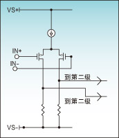
Figure 1: Basic op amp input stage.
For example, for current sensing or voltage sensing applications (such as EKG), the quality of the design is directly related to the signal voltage range that can be handled. The standard rail-to-rail op amp topology can meet this challenge. This topology has two input stages (as shown in Figure 2). When the input voltage is close to the low voltage rail, the PMOS transistor pair amplifies the signal. Conversely, the NMOS differential pair amplifies the input signal close to the upper voltage rail. In this way, the input voltage range can be the entire power supply voltage range. The most obvious trade-off for this improvement in input voltage range is the need for additional power supplies to bias the complementary differential pair.
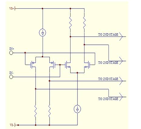
Figure 2: Dual input stage with rail-to-rail operation.
There is a less obvious tradeoff with bias voltage relative to input bias voltage. The bias of the NMOS pair does not have to match the bias of the PMOS pair - the bias is reversed when it occurs. There is a switch from one pair to the other near the middle of the supply voltage. During the switch, the bias voltage is the average of the bias voltages of each pair. This results in a staircase characteristic (as shown in Figure 3). To provide more insight, the bias voltage is plotted against temperature. The PMOS input pair activated with a low common-mode input voltage exhibits a wide range of bias voltages versus temperature. The variation in the NMOS pair results in the distribution on the right side of the figure for high common-mode input voltages.
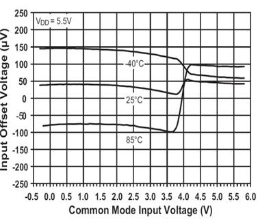
Figure 3: Input bias voltage relative to input common-mode voltage.
As mentioned earlier, in sensing applications such as EKG, any change in bias voltage will affect the accuracy of the system. The signal must first be amplified to a level far above the bias voltage to utilize a rail-to-rail amplifier like the topology shown in Figure 2.
In applications where high accuracy and low power are required, a new type of rail-to-rail amplifier is needed. The goal is to obtain a full range of input voltages without crossover bias voltage distortion, which occurs during switching in a dual differential design. Let's return to the single differential design. The input range of the topology shown in Figure 1 does not support full range input operation. A portion of the input range is reserved for biasing the current source in the saturation region. Can the current source be biased in a way that allows the input to cross between the supply rails? Input range enhancement circuitry is included in op amps such as the EL8178 to adjust the internal bias provided to the current source. Figure 4 shows this innovative topology. In the enhancement circuit is a charge pump. Although charge pumps often cause noise problems, the charge pump operates at a frequency far beyond the bandwidth of the amplifier. Therefore, the noise performance of the amplifier is not significantly changed.
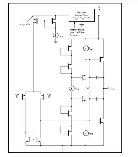
Figure 4: Rail-to-rail input stage with input range enhancement circuit
In addition, we must reconsider the issue of bias voltage. Figure 5 achieves the goal of maintaining bias voltage. The input range enhancement circuit allows a single op amp pair to provide rail-to-rail operation without the need for an additional complementary differential pair. The bias voltage is completely determined by the mismatch of only one set of transistors, so there is no crossover region. Careful layout and trimming can ensure that the input reference bias voltage is less than 100V.
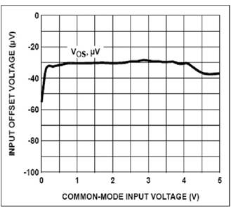
Figure 5: Enhanced input rail-to-rail level input bias voltage relative to input common-mode voltage.
So far, our discussion has been limited to MOSFET implementations. Bipolar technology can also benefit from this configuration. In addition to improving the bias voltage, the bipolar implementation can also show similar improvements in input bias current. The input bias current is only provided to one matched differential pair, rather than two differential pairs with a crossover region.
This is the evolution of the rail-to-rail amplifier. The basic input stage consisting of a single differential pair does not allow the full range of input voltages. The dual differential pair extends the input voltage range to the supply voltage, but the bias voltage (and bias current in the BJT) has nonlinearity due to the switching between the two pairs. The third solution includes an internal enhancement circuit to adjust the current source bias of the single differential pair to achieve rail-to-rail operation under the condition of continuous bias voltage. Table 1 summarizes the performance of the three example op amps. The final version, the EL8178, provides the specifications required for low-power, high-resolution systems such as portable EKG machines.
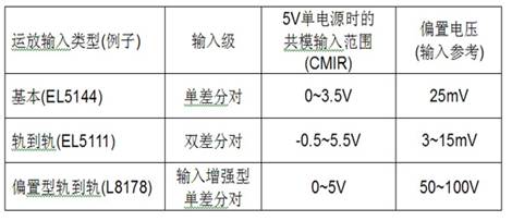
Table 1: Performance characteristics of op amps with three different input stages.
Previous article:Power Amplifier Design Based on Small Signal S Parameters
Next article:Design of power amplifier for power carrier output
Recommended ReadingLatest update time:2024-11-17 00:54


- Popular Resources
- Popular amplifiers
-
 Optimization design of SGT_MOSFET peak oscillation in synchronous rectification circuit
 -
 Study on the Behavioral Model of Silicon Carbide MOSFET Power Module and EMI Prediction of Low-Voltage Auxiliary Power Supply
 -
 Theory and practice of small-size MOS device models for VLSI simulation
 -
 Power Electronics Technology 2nd Edition (Li Jie, Chao Xiaojie, Jia Weijuan, Yang Jiayi, Lai Wei)
- High signal-to-noise ratio MEMS microphone drives artificial intelligence interaction
- Advantages of using a differential-to-single-ended RF amplifier in a transmit signal chain design
- ON Semiconductor CEO Appears at Munich Electronica Show and Launches Treo Platform
- ON Semiconductor Launches Industry-Leading Analog and Mixed-Signal Platform
- Analog Devices ADAQ7767-1 μModule DAQ Solution for Rapid Development of Precision Data Acquisition Systems Now Available at Mouser
- Domestic high-precision, high-speed ADC chips are on the rise
- Microcontrollers that combine Hi-Fi, intelligence and USB multi-channel features – ushering in a new era of digital audio
- Using capacitive PGA, Naxin Micro launches high-precision multi-channel 24/16-bit Δ-Σ ADC
- Fully Differential Amplifier Provides High Voltage, Low Noise Signals for Precision Data Acquisition Signal Chain
- Innolux's intelligent steer-by-wire solution makes cars smarter and safer
- 8051 MCU - Parity Check
- How to efficiently balance the sensitivity of tactile sensing interfaces
- What should I do if the servo motor shakes? What causes the servo motor to shake quickly?
- 【Brushless Motor】Analysis of three-phase BLDC motor and sharing of two popular development boards
- Midea Industrial Technology's subsidiaries Clou Electronics and Hekang New Energy jointly appeared at the Munich Battery Energy Storage Exhibition and Solar Energy Exhibition
- Guoxin Sichen | Application of ferroelectric memory PB85RS2MC in power battery management, with a capacity of 2M
- Analysis of common faults of frequency converter
- In a head-on competition with Qualcomm, what kind of cockpit products has Intel come up with?
- Dalian Rongke's all-vanadium liquid flow battery energy storage equipment industrialization project has entered the sprint stage before production
- Allegro MicroSystems Introduces Advanced Magnetic and Inductive Position Sensing Solutions at Electronica 2024
- Car key in the left hand, liveness detection radar in the right hand, UWB is imperative for cars!
- After a decade of rapid development, domestic CIS has entered the market
- Aegis Dagger Battery + Thor EM-i Super Hybrid, Geely New Energy has thrown out two "king bombs"
- A brief discussion on functional safety - fault, error, and failure
- In the smart car 2.0 cycle, these core industry chains are facing major opportunities!
- The United States and Japan are developing new batteries. CATL faces challenges? How should China's new energy battery industry respond?
- Murata launches high-precision 6-axis inertial sensor for automobiles
- Ford patents pre-charge alarm to help save costs and respond to emergencies
- New real-time microcontroller system from Texas Instruments enables smarter processing in automotive and industrial applications
- EEWORLD University Hall----Live Replay: Supporting 'Dual Carbon' - ADI Smart Factory Solution
- Multi-clock design strategy for FPGA in large-scale design.pdf
- [Mil MYD-YA15XC-T Review] + Unboxing and Power-on Test
- The first case in China! A 72-year-old high-level paraplegic patient eats fried dough sticks and plays mahjong with his mind. Zhejiang University's brain-computer interface has achieved many firsts
- I made a website to download Keil, Cube and other resources. Does anyone want to try it? It's free and has no speed limit.
- Does leaving the charger plugged into the socket consume electricity?
- Choosing the Right RF Transceiver IC
- Let’s talk about understanding diode parameters. What key parameters do engineers need to know when designing?
- Common impedance matching methods
- Application of digital control system in smart home field

 Optimization design of SGT_MOSFET peak oscillation in synchronous rectification circuit


 京公网安备 11010802033920号