LD (laser diode) not only has the characteristics of high monochromaticity, high coherence, high directionality and collimation of general lasers, but also has the characteristics of small size, light weight, low voltage drive, direct modulation, etc., so it is widely used in national defense, scientific research, medical treatment, optical communication and other fields. However, since LD is a device with high power density and extremely high quantum efficiency, it has poor tolerance to electrical shocks. Small current fluctuations will lead to great changes in optical power output and changes in device parameters. These changes directly endanger the safe use of the device. Therefore, in practical applications, there are very high requirements for the performance and safety protection of the driving power supply. In the design process of the driving power supply, safe and effective protection of LD is also considered, such as preventing surge shocks, slow start and other problems.
1 Circuit structure and principle
LD works by direct carrier injection. The stability of the injected current has a direct and obvious impact on the output of the laser. Therefore, the LD driver power supply needs to provide a constant current with small ripple and few glitches for the LD. The LD driver power supply consists of 4 parts: reference voltage source, constant current source circuit, pulse control circuit, and protection circuit. The structural block diagram is shown in Figure 1.

1.1 Reference voltage source circuit
The reference voltage source circuit is shown in Figure 2. Its function is to provide a high-precision, low-temperature drift voltage reference for the constant current source circuit, and at the same time, provide a stable operating voltage for the integrated circuits in the circuit (such as optocouplers, operational amplifiers, inverters, etc.).

LM317 is a three-terminal adjustable positive regulator integrated circuit from National Semiconductor Corporation of the United States. The output voltage range is 1.2 to 37 V, the maximum load current is 1.5 A, and it is easy to use. Its working process is as follows: The output voltage Vout charges C2 through R1 and VQ1. At the beginning, VQ1 is saturated and turned on, and Vout is the lowest (about 1.5 V). As the voltage on C2 increases, VQ1 gradually exits saturation and tends to be cut off, and Vout gradually increases to the rated voltage. Changing the constants of R1 and C2 can change the soft start time. Changing the value of the variable resistor R2 can adjust the value of the output voltage Vout. VD1 is used to quickly discharge the charge on C2 after shutdown. Its output voltage is:

1.2 Constant current source circuit
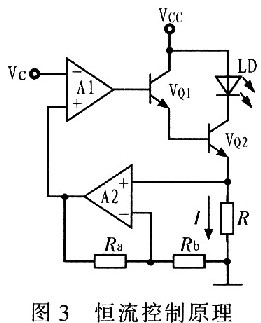
In order to achieve high current stability, most drive circuits use negative feedback control methods, and the constant current control principle is shown in Figure 3. The current stabilization circuit consists of a reference voltage circuit, a voltage-current conversion circuit, a constant current output circuit, and a feedback circuit. When the circuit is working, the reference voltage is appropriately amplified and sent to the non-inverting terminal of the operational amplifier A1. The operational amplifier A1 controls the size of the base current of VQ1 to obtain the corresponding output current. The output current generates a sampling voltage on the sampling resistor R. The sampling voltage is amplified by A2 and fed back to the inverting input terminal of the voltage amplifier A1 as a feedback voltage, and compared with the voltage at the non-inverting input terminal, the output voltage is adjusted, and then the output current of the base of VQ1 is adjusted, so that the entire closed-loop feedback system is in a dynamic balance to achieve the purpose of stabilizing the output current.

The relationship between the output current I and the set reference voltage Vc can be obtained from the negative feedback principle:

where Vc is the reference voltage, Ra and Rb are the resistors in the feedback network, and R is the sampling resistor. Under ideal circumstances, R, Ra, and Rb are constant.
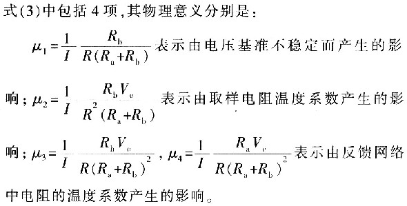
From equation (2), we can see that the output current I is linearly related to the reference voltage Vc. However, in actual situations, the temperature coefficient of the resistor and the temperature coefficient of the reference voltage will affect the stability of the output current. By fully differentiating equation (2) and simplifying it, we can get the expression of current stability:


Since the selected sampling resistor R is in the ohm level, and (Ra+Rb) is in the tens of kilo-ohm level, we have: μ2>μ1>μ3≈μ4, which shows that the main factors affecting the stability of the output current are the temperature coefficient of the sampling resistor and the stability of the voltage reference. In this constant current source, the sampling resistor accuracy is 0.1%, the temperature coefficient is ±2.5×10⁻⁵/℃, and the temperature coefficient of the voltage reference is less than 1×10⁻⁶/℃.
1.3 Pulse control circuit
For many LD applications, pulsed output is sometimes desirable because the LD junction heats very little during pulsed output. LD operation at low duty cycle and short pulse width allows pulsed current levels much higher than CW current levels, and most do not require cooling.
The key to pulse LD power supply control technology lies in the control of the current pulse waveform. The external control modulation signal adopts TTL square wave, and the LD output follows the control signal in a switching manner.

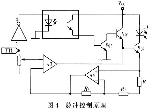
According to the above design idea, a pulse control interface circuit is designed, and its schematic diagram is shown in Figure 4. It consists of a NOT gate unit, a transistor VQ3, and a photocoupler. When the pulse is high, the NOT gate outputs a low voltage, which cuts off the photocoupler, and the photocoupler outputs a low level, which cuts off the transistor VQ3. The collector of VQ3 outputs a high level to turn on VQ1 and VQ2, and the LD works normally; on the contrary, the photocoupler is turned on, which turns on VQ3, and the collector of VQ3 outputs a low level, which cuts off VQl and VQ2, and the LD does not work. When there is no external control pulse control signal, the interface is suspended, the NOT gate inputs a high level, outputs a low voltage, the photocoupler does not work, the transistor VQ3 is cut off, and the collector of VQ3 is high, which turns on VQ1 to ensure the normal and continuous light emission of LD.
1.4 Protection circuit
Considering the vulnerability of LD, the design of protection circuit is also a very important aspect in the current control. In this design, an integrated DC voltage regulator with small supply voltage fluctuation and internal slow start, overcurrent, overheat protection, and peak current limiting functions is selected. Only an ordinary diode is connected in reverse parallel at both ends of LD to prevent reverse overvoltage, and a small-capacity capacitor is connected in parallel to prevent loop current glitches from damaging the die.
2 Results and Analysis
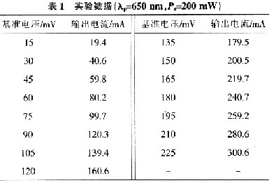
Table 1 is the test results of the reference voltage and output current when the circuit drives the LD with a wavelength of 650 nm and a power of 200 mW to work continuously. The voltage-current relationship is shown in Figure 5.

The results in FIG5 show that the reference voltage is directly proportional to the output current. By adjusting the reference voltage, the output power of the LD can be changed, that is, the output power of the LD is continuously adjustable.


Figure 6 shows the pulse waveform output by the driver. The Input curve is the input control pulse signal, and the Output curve is the voltage pulse on the LD. The results show that the rise and fall times of the voltage pulse on the LD are very short, and the stability of the voltage in the middle section makes the output current constant. The constant current amplitude ensures the stability of the LD output power. By changing the frequency and pulse width of the input pulse, the required LD laser pulse signal can be obtained.
3 Conclusion
A design method for a semiconductor laser driver power supply that can be used for continuous or pulsed output is proposed. Test results show that: 1) the drive wavelength range is 650-980 nm; 2) the output power is continuously adjustable from 0 to 300 mW; 3) continuous or pulsed output is optional. The power supply is stable, reliable, simple to control, and the power is continuously adjustable. It can be widely used in applications that require a small size of semiconductor laser driver power supply.
Previous article:Data Acquisition System Based on Printer Parallel Interface
Next article:Hardware system design of multi-sensor intelligent wheelchair
- High signal-to-noise ratio MEMS microphone drives artificial intelligence interaction
- Advantages of using a differential-to-single-ended RF amplifier in a transmit signal chain design
- ON Semiconductor CEO Appears at Munich Electronica Show and Launches Treo Platform
- ON Semiconductor Launches Industry-Leading Analog and Mixed-Signal Platform
- Analog Devices ADAQ7767-1 μModule DAQ Solution for Rapid Development of Precision Data Acquisition Systems Now Available at Mouser
- Domestic high-precision, high-speed ADC chips are on the rise
- Microcontrollers that combine Hi-Fi, intelligence and USB multi-channel features – ushering in a new era of digital audio
- Using capacitive PGA, Naxin Micro launches high-precision multi-channel 24/16-bit Δ-Σ ADC
- Fully Differential Amplifier Provides High Voltage, Low Noise Signals for Precision Data Acquisition Signal Chain
- Innolux's intelligent steer-by-wire solution makes cars smarter and safer
- 8051 MCU - Parity Check
- How to efficiently balance the sensitivity of tactile sensing interfaces
- What should I do if the servo motor shakes? What causes the servo motor to shake quickly?
- 【Brushless Motor】Analysis of three-phase BLDC motor and sharing of two popular development boards
- Midea Industrial Technology's subsidiaries Clou Electronics and Hekang New Energy jointly appeared at the Munich Battery Energy Storage Exhibition and Solar Energy Exhibition
- Guoxin Sichen | Application of ferroelectric memory PB85RS2MC in power battery management, with a capacity of 2M
- Analysis of common faults of frequency converter
- In a head-on competition with Qualcomm, what kind of cockpit products has Intel come up with?
- Dalian Rongke's all-vanadium liquid flow battery energy storage equipment industrialization project has entered the sprint stage before production
- Allegro MicroSystems Introduces Advanced Magnetic and Inductive Position Sensing Solutions at Electronica 2024
- Car key in the left hand, liveness detection radar in the right hand, UWB is imperative for cars!
- After a decade of rapid development, domestic CIS has entered the market
- Aegis Dagger Battery + Thor EM-i Super Hybrid, Geely New Energy has thrown out two "king bombs"
- A brief discussion on functional safety - fault, error, and failure
- In the smart car 2.0 cycle, these core industry chains are facing major opportunities!
- The United States and Japan are developing new batteries. CATL faces challenges? How should China's new energy battery industry respond?
- Murata launches high-precision 6-axis inertial sensor for automobiles
- Ford patents pre-charge alarm to help save costs and respond to emergencies
- New real-time microcontroller system from Texas Instruments enables smarter processing in automotive and industrial applications
- 【Portable Environmental Status Detector】Work Submission
- Development Background and Characteristics of 5G Industrial Gateway in the Internet of Things
- MSP430 FRAM Technology – How-tos and Best Practices
- ESP32-CAM Video Surveillance Robot
- Ask the Experts | Confused about DC-DC selection? MPS can help you solve it!
- A comprehensive analysis of dipole antennas
- MicroPython Hands-on (29) - SIoT of the Internet of Things
- 【Smart water cup holder】06-Work submission
- Here the role of the voltage regulator + diode combination
- Bluetooth bracelet master control selection

 LIDAR – A new (self-driving) vehicle for introducing optics to broader engineering and non-engineeri
 開關電源專業英語


 京公网安备 11010802033920号