How to Design a Programmable Gain Instrumentation Amplifier for Wideband Precision Signal Chains
Precision data acquisition subsystems are typically composed of high-performance discrete linear signal chain blocks for measurement and protection, conditioning and acquisition, or synthesis and driving. When hardware designers develop these data acquisition signal chains, they typically require high input impedance to directly interface with a variety of sensors. In this case, programmable gain is often required to adapt the circuit to different input signal amplitudes—unipolar or bipolar and single-ended or differential signals with variable common-mode voltages. Most PGIAs traditionally consist of single-ended outputs that cannot directly drive ADCs based on fully differential, high-precision SAR architectures at full speed, requiring at least one signal conditioning or driver stage amplifier. The industry continues to evolve rapidly as people focus more on providing differentiated system solutions through system software and applications. However, due to tight R&D budgets and time-to-market constraints, there is less time to build analog circuits and prototype them to verify their functionality. This puts more pressure on hardware development resources and requires further reduction in design iterations. This article will describe the key considerations when designing a discrete, wideband, fully differential PGIA and demonstrate the precision performance of the PGIA when driving a high-speed signal chain μModule® data acquisition solution.
PGIA Design Description
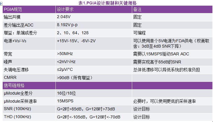
Figure 1 shows a block diagram of a simplified discrete wideband fully differential PGIA circuit. See Table 1 for key specifications and design requirements for this PGIA circuit.

Figure 1. Simplified PGIA circuit block diagram
This discrete PGIA is built using the following parts:
► ADA4898-1 low noise, high speed amplifier
► LT5400 four-channel matched resistor network used as gain and feedback resistors to set the PGIA gain
► ADG1209 low capacitance iCMOS™ multiplexer for controlling PGIA gain
► ADA4945-1 Wideband Fully Differential Amplifier (FDA)
This wideband PGIA circuit was chosen to use the above discrete components to meet the PGIA specifications highlighted in Table 1 to achieve optimized ac and dc performance when driving a fully differential high speed signal chain μModule data acquisition solution (such as the ADAQ23875 and ADAQ23878) and ADC (such as the LTC2387-16/LTC2387-18).
Design Tips and Component Selection
The ability of this wideband discrete PGIA solution to drive a signal chain μModule solution based on a high speed SAR architecture and achieve optimized performance depends on key specifications of the amplifier and FDA, such as bandwidth, slew rate, noise, and distortion. The ADA4898-1 and ADA4945-1 were chosen because their gain-bandwidth product (GBW) supports the overall bandwidth requirements of the signal chain. The ADA4945-1 (FDA) is only required when driving an ADC such as the LTC2387-16/LTC2387-18. The criteria for setting the PGIA gain depends on the selected amplifier, feedback resistors, and multiplexer, which are discussed in detail below.
Setting the PGIA Gain
Choose gain and feedback resistors
The gain resistors and feedback resistors of the amplifier should be precisely matched. The LT5400 four-channel resistor network provides 0.2ppm/°C matching drift and 0.01% resistor matching over a wide operating temperature range, with a common-mode rejection ratio (CMRR) that is better than independent matching resistors. The gain resistors around the FDA also need to be precisely matched to achieve optimized CMRR performance.
The LT5400 resistor network is used to set the gain of the amplifier. The gain calculation is shown in Equation 1 to Equation 3.

When using the LT5400, by setting R1=R4 and R2=R3, the gain is:
The gain of the amplifier and the FDA (fixed gain of 2) make up the total gain of the PGIA, as shown in Table 2.
The LT5400 family offers a variety of resistor options, as shown in Table 2. The ADG1209 multiplexer can be bypassed using an amplifier in a unity-gain configuration, so the total PGIA setting is 2 in this example.

To set the gain higher than 20, add an external precision matched gain resistor (RGAIN) between the inverting inputs of the two ADA4898-1 amplifiers and use the LT5400-4 as the feedback resistor to achieve the target gains of 64 and 128, as shown in Figure 2.
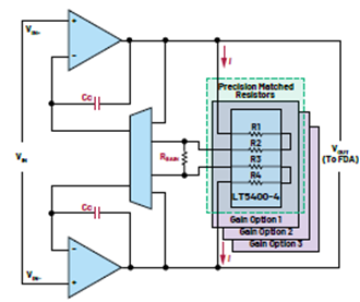
Figure 2. Multiplexer, LT5400, and RGAIN resistor set PGIA gain.
To calculate the RGAIN value, refer to Equations 4 to 8.

To achieve the desired gain, the value of RGAIN should be:

Select multiplexer
Using a multiplexer, multiple gains of this PGIA circuit can be controlled by selecting the LT5400 four-channel resistor network. When selecting a multiplexer for this wideband discrete PGIA design, several important parameters of the multiplexer should be considered, such as the on-resistance (RON), on-capacitance (CON), and off-capacitance (COFF). The ADG1209 multiplexer is recommended for this wideband PGIA design. Adding a compensation capacitor (Cc) in the feedback path of the amplifier will minimize the high frequency peaking of the gain frequency response (improve the stability of the amplifier) and reduce the impact of the on/off capacitance of the multiplexer. Cc, together with RON, the feedback resistor, and the gain resistor, will form a pole that will compensate for the impact of the zero created by the parasitic capacitance in the feedback loop gain. The value of Cc should be optimized to achieve the desired closed-loop response. When a higher feedback resistor value is used in the ADA4898-1 circuit, higher peaking will appear in the closed-loop gain frequency response due to its high input capacitance (the ADA4898-1 has an input common-mode capacitance of 2.5pF and a differential-mode capacitance of 3.2pF). To avoid this problem, a higher feedback resistor in the ADA4898-1 needs to be connected in parallel with a feedback capacitor. As shown in Figure 2, the optimized Cc value of 2.7pF recommended in the ADA4898-1 data sheet is selected here. When a smaller Cc is used, the gain frequency response has a higher peaking, but if a Cc that is too large is used, the gain flatness of the closed-loop gain is affected.
PGIA Power Supply
Figure 3 shows the evaluation board used to evaluate the performance of this discrete, wide-bandwidth PGIA design.
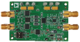
Figure 3. Discrete wide-bandwidth PGIA evaluation board
The PGIA front end, which consists of two high-speed ADA4898-1 amplifiers and an ADG1209 multiplexer, requires a ±15V power supply to drive it, while the ADA4945-1 FDA requires a 6V and 2V power rail to achieve optimal signal chain performance. Although this board requires a bench power supply, ADI recommends the LTpowerPlanner® power rail tree structure design for this PGIA circuit, which also shows the load current of each power rail, as shown in Figure 4.
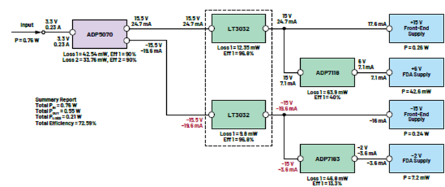
Figure 4. Recommended power tree
PGIA Performance
Bandwidth
Figure 5 shows a plot of closed-loop gain versus frequency for different gain settings. As the PGIA gain increases from 2 to 128, its bandwidth decreases and its output-referred (RTO) noise increases; therefore, the signal-to-noise ratio (SNR) decreases.
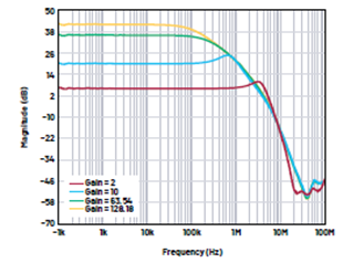
Figure 5. Bandwidth vs. frequency
CMRR
Figure 6 shows a plot of CMRR vs. frequency for different PGIA gain settings.
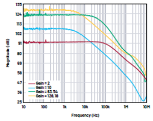
Figure 6. CMRR vs. frequency
Distortion
An Audio Precision® (APX555) signal analyzer was used to test the distortion performance of the PGIA board (Figure 4) by applying different input voltages at different gain settings, setting its output to 8.192V pp. Figure 7 shows the total harmonic distortion (THD) vs. frequency performance of the discrete wideband PGIA.
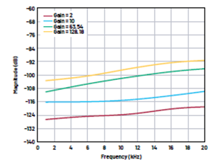
Figure 7. PGIA THD vs. frequency
Key Specifications Summary
Table 3 lists key PGIA specifications such as bandwidth, slew rate, drift, and distortion measured on a test bench using a discrete PGIA evaluation board (Figure 4).

PGIA μModule Solutions for Driving Signal Chains
Figure 8 shows the selected multiplexer as the gain input of two low noise, high speed amplifiers ADA4898-1 in parallel with the LT5400 precision resistor network to form a wideband PGIA that can drive the ADAQ23875 signal chain with a 15MSPS sampling rate uModule. The ADAQ23875 contains an internal fully differential amplifier; therefore, the FDA module in the broadband discrete PGIA evaluation board (Figure 4) should be bypassed. The Audio Precision (APx555) signal source is used to evaluate the SNR and THD, and in this example, the input amplitude is set to approximately -0.5dBFS.

Figure 8. Simplified signal chain for a discrete PGIA driving the ADAQ23875.
Complete Signal Chain Performance
Noise
Refer to Table 4 for the dynamic range and input-referred (RTI) noise for the complete signal chain (Figure 8) at specific input ranges or gain settings.

A plot of the SNR performance vs. frequency of the discrete PGIA driving the ADAQ23875 using the ADA4898-1 amplifier is shown in Figure 9. As the gain of the PGIA increases, the overall dynamic range or SNR decreases due to the noise of the individual resistors, amplifier, and the μModule solution itself.
The high precision performance of the ADAQ23878, combined with a high sampling rate, reduces noise and enables oversampling to achieve very low RMS noise and detect small amplitude signals over a wide bandwidth. In other words, the 15MSPS sampling rate greatly relaxes antialiasing filter requirements and maximizes bandwidth when digitizing fast transients and small signal levels. Oversampling refers to sampling much faster than twice the signal bandwidth (which is necessary to meet the Nyquist criterion). For example, oversampling the ADAQ23875 by 4 times provides an additional 1 bit of resolution, or 6 dB of additional dynamic range, or in other words, the improvement in dynamic range due to this oversampling is defined as: ΔDR = 10 × log10 (OSR) in dB. The typical dynamic range of the ADAQ23875 is 91 dB at 15MSPS, with a 4.096V reference and its inputs shorted to ground. For example, when the ADAQ23875 is oversampled 256 times, this corresponds to a signal bandwidth of 29.297kHz and a dynamic range of nearly 111dB (for different gain options), so small signals in the μV range can be accurately detected. Additional oversampling can be applied to trade off noise and bandwidth to accommodate the measurement being performed.
Previous article:How to Use Zero-Drift Amplifiers in Wide-Bandwidth Applications
Next article:STMicroelectronics comprehensively improves the performance of industrial and automotive op amps
Recommended ReadingLatest update time:2024-11-16 10:29


- Popular Resources
- Popular amplifiers
-
 Operational Amplifier Practical Reference Handbook (Edited by Liu Changsheng, Zhao Mingying, Liu Xu, etc.)
 -
 A Complete Illustrated Guide to Operational Amplifier Applications (Written by Wang Zhenhong)
 -
 Design of isolated error amplifier chip for switching power supply_Zhang Rui
 -
 DAM medium wave transmitter high frequency power amplifier module test platform_Tian Tian
- High signal-to-noise ratio MEMS microphone drives artificial intelligence interaction
- Advantages of using a differential-to-single-ended RF amplifier in a transmit signal chain design
- ON Semiconductor CEO Appears at Munich Electronica Show and Launches Treo Platform
- ON Semiconductor Launches Industry-Leading Analog and Mixed-Signal Platform
- Analog Devices ADAQ7767-1 μModule DAQ Solution for Rapid Development of Precision Data Acquisition Systems Now Available at Mouser
- Domestic high-precision, high-speed ADC chips are on the rise
- Microcontrollers that combine Hi-Fi, intelligence and USB multi-channel features – ushering in a new era of digital audio
- Using capacitive PGA, Naxin Micro launches high-precision multi-channel 24/16-bit Δ-Σ ADC
- Fully Differential Amplifier Provides High Voltage, Low Noise Signals for Precision Data Acquisition Signal Chain
- Innolux's intelligent steer-by-wire solution makes cars smarter and safer
- 8051 MCU - Parity Check
- How to efficiently balance the sensitivity of tactile sensing interfaces
- What should I do if the servo motor shakes? What causes the servo motor to shake quickly?
- 【Brushless Motor】Analysis of three-phase BLDC motor and sharing of two popular development boards
- Midea Industrial Technology's subsidiaries Clou Electronics and Hekang New Energy jointly appeared at the Munich Battery Energy Storage Exhibition and Solar Energy Exhibition
- Guoxin Sichen | Application of ferroelectric memory PB85RS2MC in power battery management, with a capacity of 2M
- Analysis of common faults of frequency converter
- In a head-on competition with Qualcomm, what kind of cockpit products has Intel come up with?
- Dalian Rongke's all-vanadium liquid flow battery energy storage equipment industrialization project has entered the sprint stage before production
- Allegro MicroSystems Introduces Advanced Magnetic and Inductive Position Sensing Solutions at Electronica 2024
- Car key in the left hand, liveness detection radar in the right hand, UWB is imperative for cars!
- After a decade of rapid development, domestic CIS has entered the market
- Aegis Dagger Battery + Thor EM-i Super Hybrid, Geely New Energy has thrown out two "king bombs"
- A brief discussion on functional safety - fault, error, and failure
- In the smart car 2.0 cycle, these core industry chains are facing major opportunities!
- The United States and Japan are developing new batteries. CATL faces challenges? How should China's new energy battery industry respond?
- Murata launches high-precision 6-axis inertial sensor for automobiles
- Ford patents pre-charge alarm to help save costs and respond to emergencies
- New real-time microcontroller system from Texas Instruments enables smarter processing in automotive and industrial applications
- Recruiting hardware test engineers Annual salary: 200,000-500,000 | Experience: more than 5 years | Work location: Shenzhen
- Supercapacitor balancing circuit
- When should you choose DC/DC and when should you choose LDO?
- Share: TI headphone amplifier positive and negative voltage design
- EEWORLD University Hall ---- Digital Image Processing Tianjin University of Technology
- What is the function of SMPS_INDUCTOR of BLUENRG-1?
- [SersorTile.box] Snoring Monitor Work Submission
- Python Steering Committee members share joy of 30th anniversary
- S/PDIF interface signal output problem
- [RISC-V MCU CH32V103 Review] IIC Hardware Test


 Operational Amplifier Practical Reference Handbook (Edited by Liu Changsheng, Zhao Mingying, Liu Xu, etc.)


 京公网安备 11010802033920号