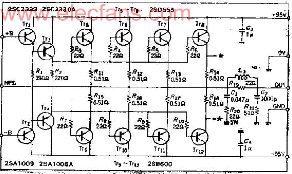
500W power amplifier output circuit that can be used for high-power unipolar power supply
Function of the circuit

This circuit is the output circuit of the power amplifier, with a load of 8 ohms, an effective output of 500W, an output voltage of 180VP-P, and an output current peak value of more than 10A, so it can also be used for high-output unipolar power supplies. The power supply voltage is positive or negative 95V, and there is no need to change the circuit parameters even if it is lower.
How the Circuit Works
When the load is 8 ohms, in order to output 500W of power, according to VCC=√8RLP, VCC should be 179V, and taking the loss voltage into account, a positive and negative 95V bipolar power supply can be used. The total collector current IO (MAX) flowing into the four parallel connections
is about 11.2A according to the formula IO (MAX) = √2PO/RL, and a power supply that can supply such a current should be equipped.
If the DC current amplification factor HFE2 of each transistor of TT5~TT12 is at least 50, then a base current of 224mA flows through it. If HFE1 of TT3 (TT4) is also 50, then the emitter current of TT1 (TT2) is about 4.5mA, and the circuit can easily work under such a current. This connection method with HFE as the multiplication result (HFE1*HFE2) is called Darlington connection.

Notes
Positive and negative bipolar power supply circuits and power supply capacity
Since the power amplifier omits the output capacitor, a bipolar power supply circuit is often used. Figure 1 shows the rectification and filtering circuit, and Figure 2 shows the regulation curve (the curve of the DC output voltage V changing with the load current IC) and the pulsation (pulse wave content) curve.
According to the required DC voltage VCC, the approximate value of the secondary voltage VCC of the power transformer is calculated, that is, VCC≈VCC*1.25 (when there is no load, VCC=√2*VCC). The current is determined by the output power and the load resistance. The average DC current IDO is calculated by the formula IDO=2IO(MAX)/π, where IO(MAX) is the maximum collector current of the output stage. The AC IAC is determined by the filter capacitors C1 and C2, which is roughly IAC=(√2~2)IDO.
The parallel capacitors C3 and C4 are used to correct the high-frequency impedance of the filter capacitor. Their capacity and type are determined according to the bandwidth to be amplified. In high-power circuits, the current flowing through is large, so pay attention to the wiring of C1 and C2. The . symbol in the figure can be used as a terminal for wiring, and try to use thick wires.

Previous article:Two-stage direct-coupled broadband amplifier with great design freedom
Next article:High voltage (120VP-P) power MOSFET amplifier
- Popular Resources
- Popular amplifiers
- High signal-to-noise ratio MEMS microphone drives artificial intelligence interaction
- Advantages of using a differential-to-single-ended RF amplifier in a transmit signal chain design
- ON Semiconductor CEO Appears at Munich Electronica Show and Launches Treo Platform
- ON Semiconductor Launches Industry-Leading Analog and Mixed-Signal Platform
- Analog Devices ADAQ7767-1 μModule DAQ Solution for Rapid Development of Precision Data Acquisition Systems Now Available at Mouser
- Domestic high-precision, high-speed ADC chips are on the rise
- Microcontrollers that combine Hi-Fi, intelligence and USB multi-channel features – ushering in a new era of digital audio
- Using capacitive PGA, Naxin Micro launches high-precision multi-channel 24/16-bit Δ-Σ ADC
- Fully Differential Amplifier Provides High Voltage, Low Noise Signals for Precision Data Acquisition Signal Chain
- LED chemical incompatibility test to see which chemicals LEDs can be used with
- Application of ARM9 hardware coprocessor on WinCE embedded motherboard
- What are the key points for selecting rotor flowmeter?
- LM317 high power charger circuit
- A brief analysis of Embest's application and development of embedded medical devices
- Single-phase RC protection circuit
- stm32 PVD programmable voltage monitor
- Introduction and measurement of edge trigger and level trigger of 51 single chip microcomputer
- Improved design of Linux system software shell protection technology
- What to do if the ABB robot protection device stops
- Why software-defined vehicles transform cars from tools into living spaces
- How Lucid is overtaking Tesla with smaller motors
- Wi-Fi 8 specification is on the way: 2.4/5/6GHz triple-band operation
- Wi-Fi 8 specification is on the way: 2.4/5/6GHz triple-band operation
- Vietnam's chip packaging and testing business is growing, and supply-side fragmentation is splitting the market
- Vietnam's chip packaging and testing business is growing, and supply-side fragmentation is splitting the market
- Three steps to govern hybrid multicloud environments
- Three steps to govern hybrid multicloud environments
- Microchip Accelerates Real-Time Edge AI Deployment with NVIDIA Holoscan Platform
- Microchip Accelerates Real-Time Edge AI Deployment with NVIDIA Holoscan Platform
- [TI High Precision Laboratory] In the course, when calculating the offset voltage error, is it not necessary to calculate the offset voltage error of the second-stage op amp?
- Does anyone know: Can one ZLL remote control control 3 ZLL lights at the same time?
- Does anyone have the Chinese version of the RL78F12 chip datasheet?
- Optimizing EMC and Efficiency in High Power DC/DC Converters Part 1
- Common Problems in RF Circuit Design
- Telink Microelectronics Matter Development Guide (I): The Past and Present of Matter
- F280049C CAN_ex3 Issue
- [Factory Visit Live Replay] Arrived at the destination - TE Qingdao Factory
- Useful tutorial | How to quickly splice PCB data at unconventional angles?
- Class AB Audio Amplifier

 UPC8182TB


 京公网安备 11010802033920号