introduce
The MAX14921 is a high-performance, high-precision battery pack measurement circuit. The improved measurement accuracy is especially important for new lithium iron phosphate batteries because the charge and discharge curves of these batteries are very flat, especially at the state of charge (SOC) of 65% to 95% of full charge. The excellent accuracy comes from the MAX14921's unique sample/hold architecture, which can minimize the battery voltage sampling error and the error caused by sampling each battery at different times.
High-precision characteristics also rely on careful circuit design. This article introduces some simple and effective layout principles to help you achieve the best accuracy indicators.
Reduce noise
The following noise-related design guidelines have become very popular in modern PCB layout. This article provides layout considerations for noise suppression in the MAX14921.
Bypass capacitor
Bypass capacitors are important circuit components. The normal operation of integrated circuits (ICs) depends on good noise filtering. In order to obtain the best characteristics, bypass capacitors should be placed as close to the power pins of the IC as possible. Table 1 lists the bypass capacitor requirements for MAX14921.
Table 1. MAX14921 bypass capacitor requirements
The capacitors can be installed on the left side of the IC, which contains the digital SPI interface, analog inputs of T1/T2/T3, analog outputs, power pins, and some sampling capacitors. To alleviate the cramped board space, the backside area of MAX14921 can be used. Vias on the PCB solder layer below MAX14921 can be used to connect signals and capacitors in this area.
Keep the distance between the capacitor and the corresponding power pin as short as possible. For some layouts, it is possible to place the capacitor on the back side of the board. If there is only one bypass capacitor, place it next to the device, such as the capacitor on pin 12 (VA).
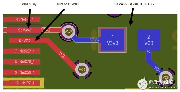
Taking a 4-layer board as an example, some layout examples are listed below. In these examples, the top layer trace is red, the second layer is DGND (green), the third layer is V5V (yellow), and the fourth layer is the bottom layer trace (blue). First, let's understand the bypass of VL, assuming that VL is 3.3V. In Figure 1, the 5th pin is connected to the back of the board through a via, and the bypass capacitor C22 is installed on the back of the board (below the MAX14921). The other pin of the capacitor is connected to the 2nd layer of the PCB, DGND, through a through hole.

Figure 1. Example of a bypass capacitor for pin 5 of the MAX14921.
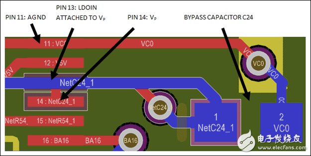
Figure 2 shows how to connect the VP bypass. Similar to pin 5, a via is used to connect the IC pin and a bypass capacitor placed on the back side. Since the return of pin 13 is AGND, the other end of C24 is connected to pin 11 instead of the DGND plane.

Figure 2. MAX14921 pin 14 bypass capacitor placement.
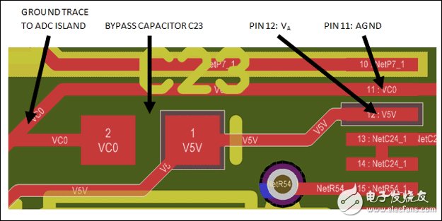
Figure 3 shows the connection of the VA bypass capacitor. As described below, it is best to run the AGND (pin 10) signal line parallel to the AOUT (pin 10) signal line. With this in mind, it is usually easier to place the bypass capacitor for pin 12 on the same side of the PCB as the MAX14921 to make full use of the bypass capacitor.

Figure 3. Bypass capacitor connection for pin 12 of the MAX14921.
ADC wiring isolation
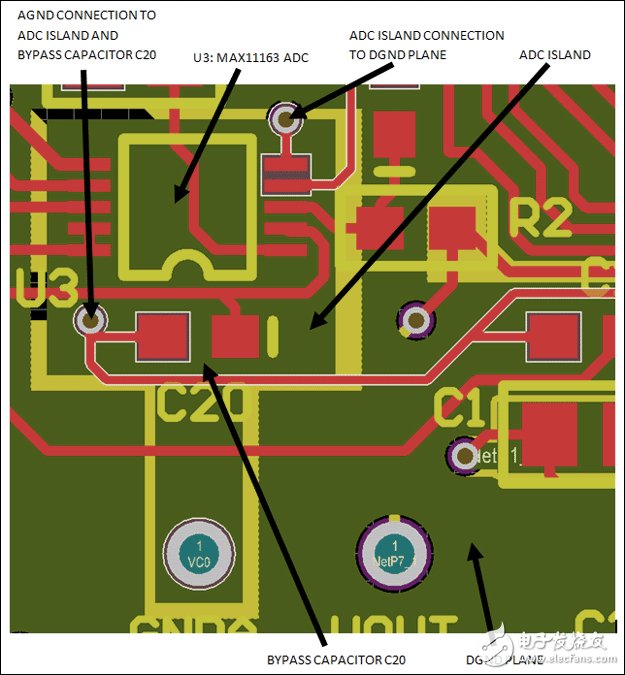
Another technique for noise management is to provide an independent ground plane underneath sensitive analog components. Figure 4 shows an example of an independent ground plane for the ADC, with U3 and pin 11 connected to this plane. The white silkscreen box highlights the vias from the left bypass capacitor C20 that connects the AGND of the MAX14921 to the independent ground plane of the ADC. This bypass capacitor is dedicated to this independent ground plane. The only connection point between the DGND and AGND planes is located at the top right of the independent ground plane of the ADC, which is shown by the white silkscreen box.

Figure 4. Ground plane isolation to the ADC (U3).
Connection between AOUT and ADC
As part of the overall solution, the MAX14921 AOUT signal (pin 10) is connected to the ADC input. Figure 5 shows a good layout example, where the AOUT lead (highlighted) has an accompanying ground (layer 2, DGND) connected to the RC filter composed of R2 and C25. In addition, the AGND lead is brought out from pin 11 in parallel with the AOUT signal line, providing a good RC filter layout. Reasonable parameters for the initial component selection of the filter are 220Ω and 220pF.

Figure 5. Connection between the AOUT pin and the ADC.
Filtering of T1, T2 and T3
Filtering the analog inputs to T1, T2, and T3 can also help improve performance. If these signals come from temperature sensors, use an RC filtering network, such as a 1kΩ resistor and a 10nF capacitor placed at the front end of the circuit to form an RC network; or a 220Ω resistor and a 2.2nF capacitor to form an RC network.
Isolation of digital signals
The MAX14921 has only a few digital signals, including: SPI interface (SCLK, SDI, SDO, and /CS), SAMPL, and EN control (if the design needs to use these two control signals). These digital signals need to be kept away from sensitive analog inputs and outputs, especially the AOUT signal (pin 10). Ideally, these digital signals are placed on different layers from the analog signals, but this requirement is not absolute if particularly strict isolation measures are taken.
Maintaining accuracy
The board layout and routing must be carefully considered to ensure that the battery voltage is accurately fed into the ADC input.
Power and signal separation
The VP pin of the MAX14921 powers the front end of the battery pack interface, which is directly connected to the top of the positive terminal of the battery pack, that is, the CV16 pin (for a 16-cell battery pack design). However, this set of leads needs to be separated from each other and the starting point should be as close to the battery end as possible. The current of each battery lead will flow through the common connection between VP and CV16, resulting in an IR voltage drop, which will cause a decrease in the accuracy of the CV16 voltage measurement.
VC0 and AGND have the same problem. The current flowing through AGND will produce an IR voltage drop in their common connection, thereby reducing the accuracy of the CV0 signal. For this reason, on the evaluation (EV) board of MAX14921, VP and CV16 use two independent pins of the connector; CV0 and AGND are also treated in the same way.
Reduce parasitic capacitance
The MAX14921 operates in two phases. The first phase charges the sampling capacitors to sample the voltage of each battery cell onto each capacitor. The second phase provides the voltage sampled by these capacitors to the ADC. In the second phase, any parasitic capacitance of the CT_ pin will reduce the voltage measurement accuracy due to charge injection.
In practice, this means that the connections between the MAX14921 and all sampling capacitors should be as short as possible, and similarly, the connections between the AOUT pin and the ADC input should also be as short as possible. Since the sampling capacitors are in 0805 packages, keeping all leads as short as possible is not an easy task.
An effective approach is to prioritize one end of the sampling capacitor and make it as close to the CT_ pin as possible. To compensate for the fact that the CB_ trace is bound to be longer, an independent ground plane is reserved under each capacitor and connected to the corresponding CB_ pin. This minimizes the parasitic capacitance generated by the leads between the sampling capacitors.
Figure 6 shows a layout example, which clearly shows the connections of the MAX14921 sampling capacitors on the bottom PCB (CT14, CB14, CT13, CB13, CT12, CB12, CT11, CB11). As can be seen from the markings in the figure, the 29th pin (CT13) is connected to its sampling capacitor with a short wire, while the lead of the 30th pin (CB13) is longer. It should be noted that CB13 is also directly connected to the independent ground plane directly below through a via.

Figure 6. Minimizing parasitic capacitance between sampling capacitors—Layer 3 (yellow) is hidden to make the picture clearer.
in conclusion
This article highlights several ways to improve PCB layout to help engineers ensure that the MAX14921 solution meets system requirements and limits measurement errors to less than 1mV.
Previous article:Programmable Gain Transimpedance Amplifiers Maximize Dynamic Range of Spectroscopy Systems (IV)
Next article:Research scheme of photoelectric tracking servo system based on MSP430 single chip microcomputer
- Popular Resources
- Popular amplifiers
- USB Type-C® and USB Power Delivery: Designed for extended power range and battery-powered systems
- ROHM develops the second generation of MUS-IC™ series audio DAC chips suitable for high-resolution audio playback
- ADALM2000 Experiment: Transformer-Coupled Amplifier
- High signal-to-noise ratio MEMS microphone drives artificial intelligence interaction
- Advantages of using a differential-to-single-ended RF amplifier in a transmit signal chain design
- ON Semiconductor CEO Appears at Munich Electronica Show and Launches Treo Platform
- ON Semiconductor Launches Industry-Leading Analog and Mixed-Signal Platform
- Analog Devices ADAQ7767-1 μModule DAQ Solution for Rapid Development of Precision Data Acquisition Systems Now Available at Mouser
- Domestic high-precision, high-speed ADC chips are on the rise
- Intel promotes AI with multi-dimensional efforts in technology, application, and ecology
- ChinaJoy Qualcomm Snapdragon Theme Pavilion takes you to experience the new changes in digital entertainment in the 5G era
- Infineon's latest generation IGBT technology platform enables precise control of speed and position
- Two test methods for LED lighting life
- Don't Let Lightning Induced Surges Scare You
- Application of brushless motor controller ML4425/4426
- Easy identification of LED power supply quality
- World's first integrated photovoltaic solar system completed in Israel
- Sliding window mean filter for avr microcontroller AD conversion
- What does call mean in the detailed explanation of ABB robot programming instructions?
- 2024 China Automotive Charging and Battery Swapping Ecosystem Conference held in Taiyuan
- State-owned enterprises team up to invest in solid-state battery giant
- The evolution of electronic and electrical architecture is accelerating
- The first! National Automotive Chip Quality Inspection Center established
- BYD releases self-developed automotive chip using 4nm process, with a running score of up to 1.15 million
- GEODNET launches GEO-PULSE, a car GPS navigation device
- Should Chinese car companies develop their own high-computing chips?
- Infineon and Siemens combine embedded automotive software platform with microcontrollers to provide the necessary functions for next-generation SDVs
- Continental launches invisible biometric sensor display to monitor passengers' vital signs
- Another technical solution for power-type plug-in hybrid: A brief discussion on Volvo T8 plug-in hybrid technology
- Integrated RF power amplifier and filter front end for wireless handsets
- [RVB2601 Creative Application Development] Graphical display and simple recognition of sound (work submission)
- TCP protocol requires restarting the circuit board for each connection
- Taiwan's semiconductor manufacturers' performance will grow slowly from July to September due to an increase in PC-related inventory
- The world is moving towards 5G. Do you think it’s time to switch to a 5G phone?
- F28335 GPIO, timer and SCI
- The value of the key resistor of the transistor voltage amplifier
- EETALK: What products might be reshaped in the 5G era? (Give away 10-100 Chip Coins)
- [Good book download] 300 examples of classic intelligent circuits!
- Allegro Issues

 TLV2442CD


 京公网安备 11010802033920号