Abstract: Based on the GPS/BD compatible high-sensitivity navigation product development and industrialization project, the classic carrier tracking loop is modified and a high-sensitivity tracking loop is designed. The traditional single-point integration data is converted into a column of data. After the FFT transformation of the data, the estimation accuracy of the carrier frequency can be improved, thereby improving the tracking sensitivity of the system. The high-sensitivity tracking loop is simulated and analyzed to prove the tracking ability of the high-sensitivity tracking loop for weak signals.
0 Introduction
The Global Navigation Satellite System (GNSS) is of great significance in many fields, including politics, economy and military. GNSS positioning technology can be seen in everything from airplanes and cars to personal handheld communication terminals. The GNSS system is widely used in the civilian field and plays an important role in national economic construction. Currently, there are four GNSS systems in use and publicly developed in the world: the GPS navigation system of the United States, the GLONASS navigation system of Russia, the GALILEO navigation system of the European Union and the BeiDou navigation system of China.
With the advancement of technology and the increase in application needs, satellite navigation has been involved in many application fields with its remarkable features such as all-weather, automation, high efficiency and high precision, as well as its unique positioning navigation, precision measurement, timing and frequency calibration and other powerful functions, making satellite navigation the third new growth point of the global IT economy after cellular mobile communications and the Internet. With the full development of the construction of the Beidou system, my country's independent satellite navigation system, the application of Beidou will be rapidly promoted, combining satellite navigation with communications, multimedia and other needs. For navigation applications for the public and industry, the development of high-performance multi-mode and high-sensitivity navigation baseband chips and multi-mode navigation baseband IP cores will improve the technical level and market share of my country's core navigation products, and provide independent core chips and solutions for major special projects and typical demonstration projects.
The GPS signal power received by the antenna is generally -130 dBm, but in complex environments such as indoors, forests, and cities, the GPS signal verification attenuation can reach 20~30 dB, and ordinary GPS receivers cannot achieve correct capture and tracking at this time. Based on the research background of high-sensitivity digital baseband chips, this paper modifies the classic carrier tracking loop and designs a high-sensitivity tracking loop design. The high-sensitivity tracking loop receiver achieves correct capture and tracking.
1 Autonomous Tracking Loop Design
1.1 Autonomous Tracking Loop Design
The satellite signal consists of three parts: navigation message, pseudo-random spread spectrum (C/A) code and carrier. The baseband signal processor synchronization process includes acquisition and tracking. Acquisition is a two-dimensional search process that roughly estimates the carrier Doppler frequency deviation and C/A code phase offset caused by the relative motion of the satellite and the receiver. After acquisition, these two parameters are used to initialize the tracking loop.
The tracking loop performs precise phase synchronization and tracking, thereby achieving carrier stripping and C/A code stripping, and ultimately obtaining the navigation message for navigation solution.
The satellite number and spread spectrum code phase in the results of the autonomous acquisition channel are input into the satellite spread spectrum code generator, which starts the generation of spread spectrum code sequences, including 3 sequences of leading 0.5 code chips, immediate code chips and lagging 0.5 code chips, and then correlated with the local pseudo code signal. Through the related operations of the spread spectrum code tracking loop and the carrier tracking loop, the carrier loop and the code loop are kept in a locked state. The program structure is shown in Figure 1.
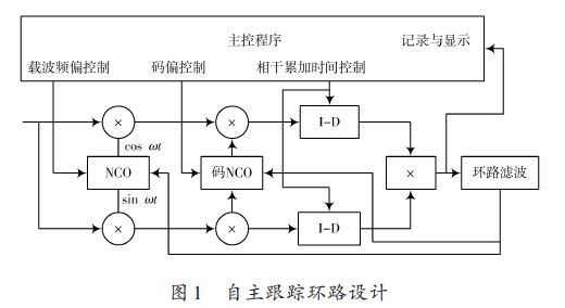
The tracking loop includes a carrier tracking loop and a code tracking loop. The two loops affect each other. Only when the two loops are locked at the same time can the navigation message be demodulated. The carrier tracking loop is more sensitive to environmental noise, crystal oscillator phase noise and dynamic stress, and is more likely to lose lock than the code tracking loop. Therefore, it becomes the key and design difficulty of the receiver.
1.2 Code Tracking Loop
Since the code tracking loop DDLL algorithm can be implemented by software and can ensure that the pseudo code delay is accurate to within 1% of the code chip, the autonomous code tracking loop adopts this method to track the pseudo code phase, that is, the local code generator is used to generate phase advance and lag signals and correlate them with the input signal, and the two branch results are compared to obtain the code phase error signal to control the code DCO and generate a local code signal consistent with the input code phase.
The input of the code loop phase detector is the related signal of the code phase advance/lag of the in-phase/orthogonal branch. When code correlation occurs, the loop enters the tracking state. Assuming d = 2δ, d is the phase interval between the phase advance and lag branches, the control quantity B (k) of the lead-lag type incoherent DDLL loop can be obtained by formula (1):
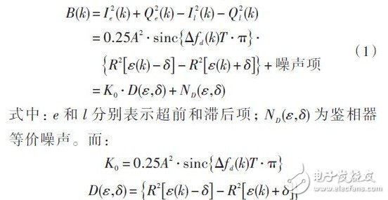
They represent the gain coefficient and phase detection characteristic function of the phase detector respectively. The code length of GPS C/A code is L = 1 023, the code length of BD C/A code is L = 2 046, the code element width is tc = 20 ms, and the correlation function is:

From this we can get the phase characteristic function of the phase detector:
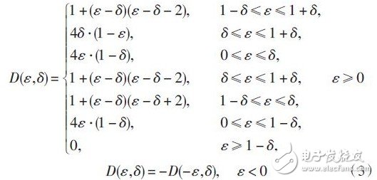
The phase detection characteristic function is a function of the correlation interval and the code phase deviation.
If (-δ, δ) is defined as the phase-locked linear range, the slope D′(ε, δ) of the phase-locked characteristic function at ε = 0 is the phase-locked gain of the DDLL loop, and Dmax (ε, δ) is the tracking traction range.
1.3 Carrier Tracking Loop Design
Carrier synchronization includes two processes: capture and tracking. Carrier capture, i.e., a rough estimate of Doppler frequency shift, is completed by the capture algorithm of the fast capture channel, while accurate carrier phase and Doppler frequency shift tracking is achieved through the feedback tracking control loop. This scheme uses a non-coherent FLL loop--CPAFC plus phase-locked tracking algorithm as a carrier tracking method. After pseudo-code capture by the capture algorithm, the carrier Doppler frequency shift range is "pulled" to 500 Hz. In order to make the Doppler frequency shift enter the linear working range of the cross-product discriminator, the algorithm first uses the cross-product discriminator to reduce the frequency from several hundred Hz to a few Hz, and then uses the phase-locked loop for accurate frequency tracking.
The frequency discrimination algorithm of the cross-product automatic frequency tracking loop is:

Assume that the modulated data bits remain unchanged during the continuous measurement process, that is, D(k)D(k - 1) = 1. The frequency offset caused by the carrier maneuvering during the pre-detection integration time can be regarded as a constant value, so Δfd ≡ Δfd (k) = Δfd (k - 1) holds. And since Φk = Δfd (k) - tk + Φ0, then:

The output is proportional to the phase change within a unit time interval, and this output can be used to control the carrier DCO to achieve the purpose of frequency tracking. The algorithm requires calculation within the same data bit, and can still achieve good performance under low signal-to-noise ratio conditions [7].
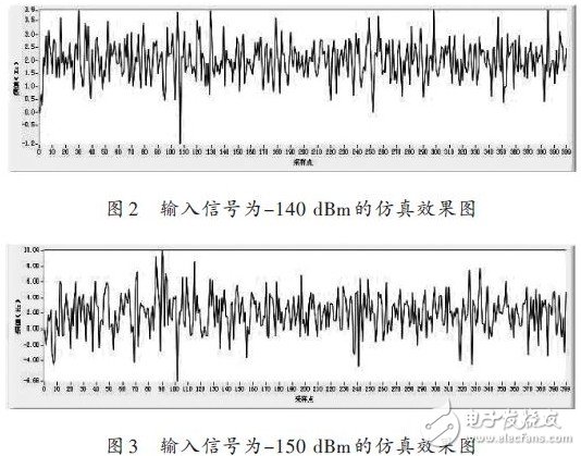
The coherent integration time is set to 20 ms, the carrier fixed frequency deviation is 2 Hz, and the loop bandwidth is 10 Hz. The simulation effect diagrams when the input signal is weakened from -140 dBm to -160 dBm are shown in Figures 2 to 5.
It can be seen from Figures 2 to 5 that when the input signal power is less than -150 dBm, the traditional loop tracking strategy can no longer achieve stable tracking, and a new tracking method must be designed.

2 Highly sensitive tracking loop design
Based on the existing baseband algorithms and circuits of multiple GPS, BD, and GLONASS receivers, the GNSS R&D platform and development board are used to further test and verify the method of improving the autonomous sensitivity of the receiver. Flexible and efficient circuit structures such as shared matching filters and correlators are used. Matching filters are used for search and capture, and correlators are used for tracking. Different channels, GPS, and BeiDou-2 share the same matching filter and correlator in time-sharing, and the circuit speed is exchanged for the circuit scale, which improves the processing capacity of the system, thereby achieving the purpose of improving capture sensitivity, reducing startup time, reducing false capture phenomena, and reducing circuit scale.
In terms of algorithm, a combination of coherent integration and incoherent integration is used to achieve weak signal capture and tracking. Coherent integration is more efficient than incoherent integration, but coherent integration is limited by bit sign inversion and will reduce the step size of frequency search. The coherent integration time is difficult to be very long, so only a combination of coherent integration and incoherent integration can be used to increase the total integration time to seconds to achieve high sensitivity.
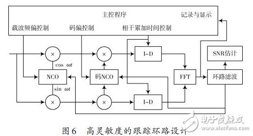
The classic carrier tracking loop is modified as shown in Figure 6. The core idea is to convert the traditional single-point integration data into a column of data. After the data is transformed by FFT, the estimation accuracy of the carrier frequency can be improved, thereby improving the tracking sensitivity of the system, and basically meeting the requirements of high-sensitivity tracking loop design. The coherent integration time PIT is set to 20 ms, the preset frequency deviation is 20 Hz, and the simulation diagrams when the input signal power is -150~-160 dBm are shown in Figures 8 and 9.

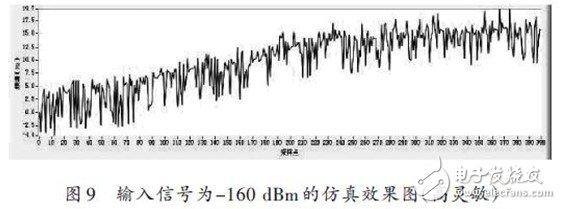
It can be seen from Figures 7 to 9 that in the case of weak signals, the loop still has a strong frequency tracking capability.
3 Conclusion
Based on the research background of digital baseband chips, this paper designs and implements GPS and BD2 carrier tracking loop design. It provides a simulation and implementation of a highly sensitive carrier tracking loop, which is the core technology for the implementation of a highly sensitive receiver.
Previous article:Teach you a few tricks to help your home appliances cool down
Next article:Design of differential Hall speed sensor using TLE4921-5U
- Popular Resources
- Popular amplifiers
- High signal-to-noise ratio MEMS microphone drives artificial intelligence interaction
- Advantages of using a differential-to-single-ended RF amplifier in a transmit signal chain design
- ON Semiconductor CEO Appears at Munich Electronica Show and Launches Treo Platform
- ON Semiconductor Launches Industry-Leading Analog and Mixed-Signal Platform
- Analog Devices ADAQ7767-1 μModule DAQ Solution for Rapid Development of Precision Data Acquisition Systems Now Available at Mouser
- Domestic high-precision, high-speed ADC chips are on the rise
- Microcontrollers that combine Hi-Fi, intelligence and USB multi-channel features – ushering in a new era of digital audio
- Using capacitive PGA, Naxin Micro launches high-precision multi-channel 24/16-bit Δ-Σ ADC
- Fully Differential Amplifier Provides High Voltage, Low Noise Signals for Precision Data Acquisition Signal Chain
- LED chemical incompatibility test to see which chemicals LEDs can be used with
- Application of ARM9 hardware coprocessor on WinCE embedded motherboard
- What are the key points for selecting rotor flowmeter?
- LM317 high power charger circuit
- A brief analysis of Embest's application and development of embedded medical devices
- Single-phase RC protection circuit
- stm32 PVD programmable voltage monitor
- Introduction and measurement of edge trigger and level trigger of 51 single chip microcomputer
- Improved design of Linux system software shell protection technology
- What to do if the ABB robot protection device stops
- Sn-doped CuO nanostructure-based ethanol gas sensor for real-time drunk driving detection in vehicles
- Design considerations for automotive battery wiring harness
- Do you know all the various motors commonly used in automotive electronics?
- What are the functions of the Internet of Vehicles? What are the uses and benefits of the Internet of Vehicles?
- Power Inverter - A critical safety system for electric vehicles
- Analysis of the information security mechanism of AUTOSAR, the automotive embedded software framework
- Brief Analysis of Automotive Ethernet Test Content and Test Methods
- How haptic technology can enhance driving safety
- Let’s talk about the “Three Musketeers” of radar in autonomous driving
- Why software-defined vehicles transform cars from tools into living spaces
- Power supply control principle of three-phase fuel pump used in Mercedes-Benz passenger cars
- Review summary: Free review of Fudan Micro FM33LG0 series, Winsilver chip
- ESP32-S2-Saola-1 calculates pi
- DCDC H-bridge circuit, what is the principle of boost and buck?
- How to measure positive and negative 1.5V signals using a single power supply system?
- [Zhongke Bluexun AB32VG1 RISC-V evaluation board] Current and voltage detection project development
- Complete list of motor model parameters, no longer worried about not understanding the motor model
- Learn about enhanced eCall car design in one article
- CC2640R2F as master control for DHT11
- Calculation of RC parameters for PWM as DAC

 INA110AG


 京公网安备 11010802033920号