Although ADCs look very simple, they must be used correctly to achieve optimal performance. ADCs have the same performance limitations as simple analog amplifiers, such as limited gain, offset voltage, common-mode input voltage limitations, and harmonic distortion. The sampling nature of ADCs requires us to consider clock jitter and aliasing more. The following guidelines can help engineers get the most out of ADCs in their designs.
Analog Input
Take the analog input signal of the ADC seriously and try to keep it clean. "Useless input" usually leads to "digital useless output". The analog signal path should be kept away from any fast switching digital signal lines to prevent noise from coupling into the analog path from these digital signal lines.
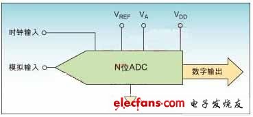
Although the simplified block diagram shows single-ended analog inputs, differential analog inputs are often used on high-performance ADCs. Driving the ADC differentially provides greater common-mode noise rejection and generally achieves better ac performance due to smaller on-chip signal swings. Differential drive is typically implemented using a differential amplifier or transformer. Transformers can provide better performance than amplifiers because active amplifiers introduce additional noise sources that affect overall performance. However, if the signal being processed has a dc component, transformers with dc blocking properties cannot be used. The noise and linearity performance of the driver amplifier must be considered when designing the pre-driver circuit. It is important to note that because high-performance ADCs typically have very high input bandwidths, filtering directly at the ADC input pins can reduce the amount of broadband noise that is mixed into the baseband.
Reference input
The reference input should be treated as another analog input and must be kept as clean as possible. Any noise on the reference voltage (VREF) is indistinguishable from noise on the analog signal. The required decoupling capacitors are specified in the data sheet of the general ADC. These capacitors should be placed as close to the ADC as possible. In order to save board area, PCB designers sometimes place decoupling capacitors on the back of the PCB, which should be avoided as much as possible because the inductance of the vias will reduce the decoupling performance of the capacitors at high frequencies. VREF is usually used to set the full-scale range of the ADC, so reducing the VREF voltage value will reduce the LSB value of the ADC, making the ADC more sensitive to system noise (the LSB value of a 1V full-scale 10-bit ADC is equal to 1V/210=1mV).

Figure 1: Typical analog-to-digital converter functional block diagram
Clock Input
Depending on the application, the digital clock input may be as important as the analog input. There are two major sources of noise in ADCs: one is caused by the quantization of the input signal (proportional to the number of bits in the ADC), and the other is caused by clock jitter (sampling the input signal at the wrong time). According to the following formula, quantization noise will limit the maximum possible signal-to-noise ratio (SNR) value in non-oversampled ADC applications.
Where N is the number of bits of the ADC and SNR is the signal-to-noise ratio.
This makes intuitive sense: for every additional bit, the total number of ADC codes doubles, and the quantization uncertainty is reduced by half (6dB). Therefore, a 10-bit ADC can theoretically provide an SNR of 61.96dB. Any jitter on the sampling clock will further degrade the SNR according to the following equation:

where SNRj is the jitter-limited SNR, fa is the analog input frequency, and tj is the root mean square (rms) value of the clock jitter.
Digitizing a 70MHz analog signal with a sampling clock that has 8ps jitter gives a jitter-limited SNR of approximately 49dB, which is equivalent to reducing the performance of a 10-bit ADC to approximately 8 bits. The clock jitter must be less than 2ps to achieve an SNR equivalent to a 10-bit ADC. There are many second-order factors that affect SNR, but the above equation is a very good first-order approximation. Differential clocks are often used to reduce jitter.
Power Input
Most ADCs have separate power inputs, one for analog circuitry and one for digital circuitry. It is recommended to use sufficient decoupling capacitors as close to the ADC as possible. Minimize the number of PCB vias and the trace length from the ADC power pins to the decoupling capacitors to minimize the inductance between the ADC and the capacitors. Just like the reference voltage decoupling, board designers sometimes place the decoupling capacitors on the back of the PCB under the chip to save board area. For the same reason, this should also be avoided. The ADC data sheet generally provides recommended decoupling solutions. In order to achieve specific performance, power and ground are often implemented using dedicated PCB layers.
Digital Output
The ADC switching digital signal output will generate transient noise and couple back to the sensitive analog circuit part in the ADC, causing failure. Shortening the output trace length to reduce the capacitive load driven by the ADC can help reduce this effect. Placing a series resistor at the ADC output can also reduce the output current spike. The ADC data sheet usually has some design recommendations for this.
Above, we introduced what ADC is, ADC's technical parameters and misunderstandings, and detailed some suggestions on how to improve ADC performance. Next, we will continue to introduce some specific design issues of ADC, ADC input noise pros and cons analysis, ADC input converter circuit analysis, ADC input impedance signal chain design, etc. We detailed the design challenges of ADC, how to move from high performance to low power consumption, and also gave a deep understanding of different types of ADC digital outputs.
ADC Input Noise Pros and Cons Analysis
In most cases, lower input noise is better, but in some cases, input noise can actually help achieve higher resolution. This may seem counterintuitive, but read on to learn why some noise is good noise.
Input Referred Noise (Code Transition Noise)
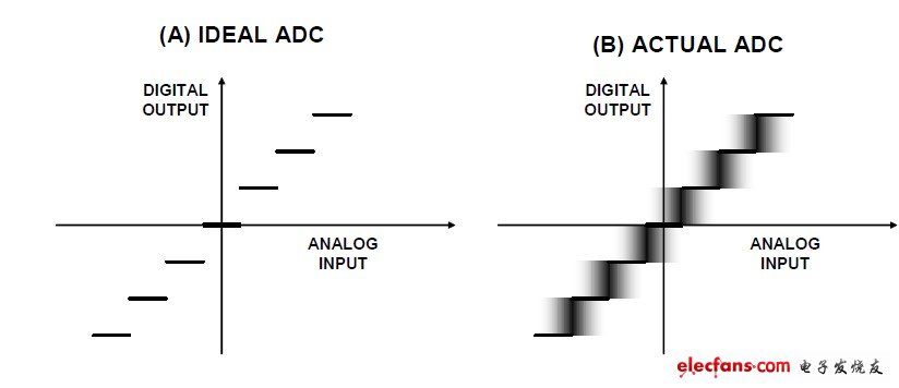
Real ADCs deviate from the ideal ADC in many ways. The input-referred noise is certainly not what it would appear to be under ideal conditions, and its effect on the overall transfer function of the ADC is shown in Figure 1. As the analog input voltage increases, the "ideal" ADC (as shown in Figure 1A) maintains a constant output code until it reaches the transition region, at which point the output code instantly jumps to the next value and remains at that value until it reaches the next transition region. In theory, the "code transition" noise of an ideal ADC is zero, and the transition region width is also equal to zero. Real ADCs have a certain amount of code transition noise, so the transition region width depends on the amount of input-referred noise (as shown in Figure 1B). Figure 1B shows a situation where the width of the code transition noise is approximately 1 LSB (least significant bit) peak-to-peak.

Figure 1: Code transition noise (input-referred noise) and its effect on the ADC transfer function
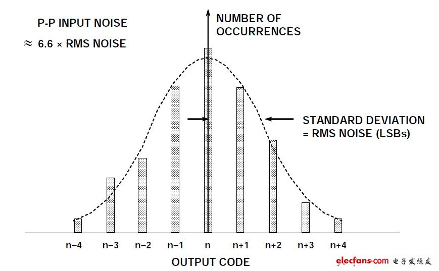
All ADCs generate some amount of root mean square (RMS) noise internally due to resistor noise and "kT/C" noise. This noise is present even for dc input signals and is the cause of code transition noise. Code transition noise is often referred to today as "input referred noise" rather than simply "code transition noise." Input referred noise is usually characterized by a histogram of several output samples when the ADC input is at dc values. The output of most high speed or high resolution ADCs is a range of codes centered around the nominal dc input value (see Figure 2). To measure its value, the ADC input is grounded or connected to a deeply decoupled voltage source, and a large number of output samples are taken and plotted as a histogram (sometimes called a "grounded input" histogram). Since the noise is roughly Gaussian, the standard deviation of the histogram, σ, can be calculated, which corresponds to the effective input rms noise. Reference 1 details how to calculate σ from the histogram data. Although this rms noise can be expressed as an rms voltage referenced to the ADC full-scale input range, the convention is to express it in LSB rms.

Figure 2: Impact of input-referred noise on the ADC's "grounded input" histogram (ADC has low DNL)
Although the inherent differential nonlinearity (DNL) of the ADC may cause its noise distribution to deviate slightly from the ideal Gaussian distribution (partial DNL is shown in the example in Figure 2), it is at least approximately Gaussian. If the DNL is large, the values should be calculated for several different DC input voltages and then averaged. For example, if the code distribution has large and unique peaks and valleys, it indicates a poor ADC design or, more likely, PCB layout errors, poor grounding, and improper power supply decoupling (see Figure 3). If the width of the distribution changes dramatically as the DC input sweeps across the ADC input voltage range, this also indicates a problem.
ADC Input Converter Circuit Analysis
Many high-precision analog-to-digital converters require an input range between 0.0V and 5.0V. For example, the MAX1402 (18-bit multichannel Σ-Δ ADC) measures the difference between two inputs. In a typical single-ended application, the ADC compares the input voltage to a fixed reference voltage (e.g., 2.500V): when ADCIN = 0V, the digital output represents 0V – 2.5V = -2.5V; when ADCIN = 2.5V, the output represents 2.5V – 2.5V = 0V; and when ADCIN = 5V, the output represents 5V – 2.5V = 2.5V. Thus, the digital output range corresponding to an ADCIN of 0V to 5V is ±2.5V.
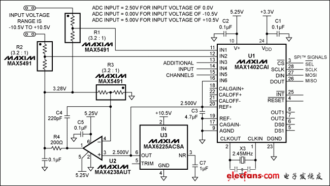
The circuit in Figure 1 converts ±10.5V input signals to the input range of the MAX1402 ADC (0V to 5V). The two channels of the ADC (IN1 and IN2 in this case) are configured for fully differential or high-precision single-ended measurements. The R1, R2 resistor divider transforms the input and biases the input with 3.28V. When the input is grounded, the ADC input is centered around 2.5V (when VIN = 0V, the ADC digital output is 0). The precision of the components ensures the 16-bit accuracy of the ADC.

Figure 1. This circuit allows an ADC with an input range of 0V to 5V (single-ended or differential) to process an input range of ±10.5V.
Configuring the MAX1402 for differential measurement allows the voltage difference between IN1 and IN2 to be measured. These inputs accept ±10.5V input voltages, and the internal programmable gain amplifier (PGA) is used to increase the resolution of small signals. For example, a gain of 4 allows the ADC to achieve 16-bit resolution when measuring ±2.625V input signals.
For single-ended measurements, the input can be configured as two independent channels and compared to the 2.50V reference voltage at IN6. For higher accuracy, the ADC can be configured as a differential input with one channel acting as a ground sense input.
The resistor divider ratio can be changed to accommodate different input ranges, but the same ratio needs to be used to bias the circuit. For example, a 5:1 ratio corresponds to a ±15.0V input range and a 3.00V bias. To calibrate the system, simply connect the input to ground, connect the input to a known voltage, and record the output value. These two values can be used to calculate the bias and gain factors for each input range.
ADC Input Impedance Signal Chain Design Summary
Understanding converter impedance is an important part of signal chain design. In short, why waste a lot of money on expensive test equipment or go through the trouble of measuring impedance if you don’t really need it? It is faster and easier to get the converter impedance curve by using the RC parallel combination impedance provided by the data sheet and a little simple calculation.
Also note that process resistor tolerances can be as high as ±20%. Even if you take the trouble to measure the input or output impedance of any device, you will only get one data point (unless, of course, you measure many devices over multiple batches over temperature and supply voltage). Use the simulated R||C values from the data sheet, which provide enough information about the characteristic impedance vs. frequency to design a signal chain that works properly.
Previous article:What analog engineers must know: Learn about analog-to-digital converters in all aspects
Next article:What analog engineers must know: Learn about analog-to-digital converters in all aspects
- High signal-to-noise ratio MEMS microphone drives artificial intelligence interaction
- Advantages of using a differential-to-single-ended RF amplifier in a transmit signal chain design
- ON Semiconductor CEO Appears at Munich Electronica Show and Launches Treo Platform
- ON Semiconductor Launches Industry-Leading Analog and Mixed-Signal Platform
- Analog Devices ADAQ7767-1 μModule DAQ Solution for Rapid Development of Precision Data Acquisition Systems Now Available at Mouser
- Domestic high-precision, high-speed ADC chips are on the rise
- Microcontrollers that combine Hi-Fi, intelligence and USB multi-channel features – ushering in a new era of digital audio
- Using capacitive PGA, Naxin Micro launches high-precision multi-channel 24/16-bit Δ-Σ ADC
- Fully Differential Amplifier Provides High Voltage, Low Noise Signals for Precision Data Acquisition Signal Chain
- Innolux's intelligent steer-by-wire solution makes cars smarter and safer
- 8051 MCU - Parity Check
- How to efficiently balance the sensitivity of tactile sensing interfaces
- What should I do if the servo motor shakes? What causes the servo motor to shake quickly?
- 【Brushless Motor】Analysis of three-phase BLDC motor and sharing of two popular development boards
- Midea Industrial Technology's subsidiaries Clou Electronics and Hekang New Energy jointly appeared at the Munich Battery Energy Storage Exhibition and Solar Energy Exhibition
- Guoxin Sichen | Application of ferroelectric memory PB85RS2MC in power battery management, with a capacity of 2M
- Analysis of common faults of frequency converter
- In a head-on competition with Qualcomm, what kind of cockpit products has Intel come up with?
- Dalian Rongke's all-vanadium liquid flow battery energy storage equipment industrialization project has entered the sprint stage before production
- Allegro MicroSystems Introduces Advanced Magnetic and Inductive Position Sensing Solutions at Electronica 2024
- Car key in the left hand, liveness detection radar in the right hand, UWB is imperative for cars!
- After a decade of rapid development, domestic CIS has entered the market
- Aegis Dagger Battery + Thor EM-i Super Hybrid, Geely New Energy has thrown out two "king bombs"
- A brief discussion on functional safety - fault, error, and failure
- In the smart car 2.0 cycle, these core industry chains are facing major opportunities!
- The United States and Japan are developing new batteries. CATL faces challenges? How should China's new energy battery industry respond?
- Murata launches high-precision 6-axis inertial sensor for automobiles
- Ford patents pre-charge alarm to help save costs and respond to emergencies
- New real-time microcontroller system from Texas Instruments enables smarter processing in automotive and industrial applications
- APM32E103 MINI development board information (software resource package, schematic diagram, user manual, etc.)
- Is there a dual Schottky diode similar to BAT54x that can pass a larger current (0.6A*2)?
- Siemens Communications' fixed network, mobile network and operator service departments have been merged into Nokia. Where will the enterprise network go?
- [RVB2601 Creative Application Development] Dynamically loading MBRE JPEG decoder transplant source code and test results
- Right angle turn without amplitude
- Intelligence at the Edge Powers Autonomous Factories
- 8. [Learning LPC1768 library functions] Timer experiment
- One minute to understand: World Industrial History (video explanation)
- EEWorld's "Search Device" applet is now online, allowing you to easily check device data and make chip selection easier
- Wireless transmission distance calculation

 Multisim Circuit System Design and Simulation Tutorial


 京公网安备 11010802033920号