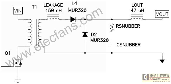
Have you ever struggled with picking snubber components? Calculating how much capacitance and resistance to add can be challenging. Here’s a quick way to solve this problem. Figure 1 shows the power stage of a forward converter. The converter is run by a transformer that couples the input voltage to the secondary circuit, which rectifies and filters the input voltage. A snubber is usually needed when D2 is forced to commutate off through a resistor that forms a low impedance circuit with the reflected primary voltage and the transformer leakage inductance. D2 can be a silicon pn diode that has a reverse recovery charge that must be depleted before it turns off. This loads up excess current in the leakage inductance, resulting in high-frequency ringing and excessive diode voltage. A similar situation exists with Schottky diodes, due to their large junction capacitance, and with synchronous rectifiers, due to their turn-off delay time.

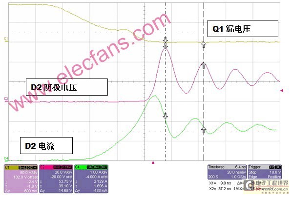
Figure 1 Leakage inductance delays D2 turning off Figure 2 shows some circuit waveforms, with the top trace being the Q1 drain voltage, the middle trace being the voltage at the junction of D1 and D2, and the bottom trace being the current through D1. In the top trace, you can see that when Q1 turns on, its drain voltage is reduced below the input voltage, which causes the diode D1 current to increase. If D2 did not have a reverse recovery charge, the junction voltage would rise when the D1 current equaled the output current. Since D2 has a reverse recovery charge, the D1 current increases further, which begins to consume the charge. Once the charge is depleted, the diode turns off, causing the increased junction voltage to increase further. Note that the current continues to increase until the junction voltage equals the reflected input voltage because there is a positive voltage across the leakage inductance. As the current increases, it charges the parasitic capacitance and causes more ringing and losses in the circuit.

Figure 2 D2 causes excessive ringing when it is off These ringing waveforms may be unacceptable because they may cause EMI problems or unacceptable voltage stress on the diode. An RC snubber across D2 can significantly reduce the ringing with little impact on efficiency. You can calculate the ringing frequency using the following equation (see Equation 1):

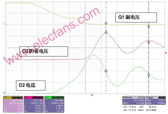
But how do you know the values of L and C in the circuit? The trick is to lower the ringing frequency by adding a known value capacitor across D2, which gives you two equations and two unknowns. Solving for these values is much easier if you add just enough capacitance to cut the ringing frequency in half. To cut the frequency in half, you need a total capacitance that is four times the parasitic capacitance you started with. Then, just divide the added capacitance by three to find the parasitic capacitance. Figure 3 shows the waveform for 470 pF of capacitance across D2 at half the original ringing frequency. Therefore, the circuit has about 150 pF of parasitic capacitance. Note that simply adding capacitance does little to the amplitude of the ringing; the circuit also needs some resistance to damp the ringing. This is another reason why a capacitance factor of 3 is a good place to start. If the resistor is chosen appropriately, it will provide excellent damping with minimal impact on efficiency. The best value for the damping resistor is almost the typical resistance of the parasitic element (see Equation 2).

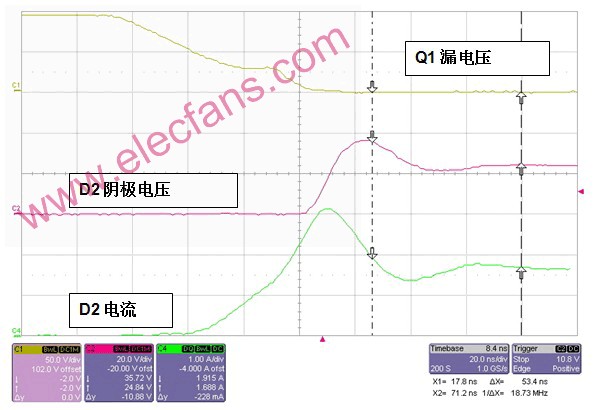
Figure 3 Completing the parasitic calculations by increasing the ringing frequency by a factor of two Using Equation 1 with a 35 MHz ringing frequency and a parasitic capacitance of 150 pF, the leakage inductance is calculated to be 150 nH. Substituting 150 nH into Equation 2 yields a snubber resistor value of approximately 30 Ohms. Figure 4 shows the effect of adding the snubber resistor. The ringing is completely eliminated and the voltage stress is reduced from 60V to 40V. This allows us to select a lower voltage rated diode, thus achieving an improvement in efficiency. The final step in the process is to calculate the snubber resistor losses. This is accomplished using Equation 3, where f is the operating frequency.
Once you have done the calculations, you need to decide if the circuit can tolerate the losses in the snubber. If not, you need to make a trade-off between ringing and snubber losses.

Figure 4. Choosing the proper snubber resistor can completely eliminate ringing. In summary, snubbering a forward converter is a simple process: 1) add capacitance to cut the ringing frequency in half; 2) calculate parasitic capacitance and inductance; 3) calculate the damping resistor and inductance; 4) determine if the circuit losses are within acceptable limits.
Previous article:Active Clamp Topology Forward Converter with Shutdown Reset Switch
Next article:Design and simulation of DDC filter based on FPGA
- Popular Resources
- Popular amplifiers
-
 Virtualization Technology Practice Guide - High-efficiency and low-cost solutions for small and medium-sized enterprises (Wang Chunhai)
 -
 Modern high-frequency switching power supply technology and its application (Liu Fengjun)
 -
 Improve Your Automotive ECU Design with a Low-IQ Buck Converter
 -
 Learn C++ in 21 Days (8th Edition) (Siddhartha Rao, Yuan Guozhong)
- High signal-to-noise ratio MEMS microphone drives artificial intelligence interaction
- Advantages of using a differential-to-single-ended RF amplifier in a transmit signal chain design
- ON Semiconductor CEO Appears at Munich Electronica Show and Launches Treo Platform
- ON Semiconductor Launches Industry-Leading Analog and Mixed-Signal Platform
- Analog Devices ADAQ7767-1 μModule DAQ Solution for Rapid Development of Precision Data Acquisition Systems Now Available at Mouser
- Domestic high-precision, high-speed ADC chips are on the rise
- Microcontrollers that combine Hi-Fi, intelligence and USB multi-channel features – ushering in a new era of digital audio
- Using capacitive PGA, Naxin Micro launches high-precision multi-channel 24/16-bit Δ-Σ ADC
- Fully Differential Amplifier Provides High Voltage, Low Noise Signals for Precision Data Acquisition Signal Chain
- Innolux's intelligent steer-by-wire solution makes cars smarter and safer
- 8051 MCU - Parity Check
- How to efficiently balance the sensitivity of tactile sensing interfaces
- What should I do if the servo motor shakes? What causes the servo motor to shake quickly?
- 【Brushless Motor】Analysis of three-phase BLDC motor and sharing of two popular development boards
- Midea Industrial Technology's subsidiaries Clou Electronics and Hekang New Energy jointly appeared at the Munich Battery Energy Storage Exhibition and Solar Energy Exhibition
- Guoxin Sichen | Application of ferroelectric memory PB85RS2MC in power battery management, with a capacity of 2M
- Analysis of common faults of frequency converter
- In a head-on competition with Qualcomm, what kind of cockpit products has Intel come up with?
- Dalian Rongke's all-vanadium liquid flow battery energy storage equipment industrialization project has entered the sprint stage before production
- Allegro MicroSystems Introduces Advanced Magnetic and Inductive Position Sensing Solutions at Electronica 2024
- Car key in the left hand, liveness detection radar in the right hand, UWB is imperative for cars!
- After a decade of rapid development, domestic CIS has entered the market
- Aegis Dagger Battery + Thor EM-i Super Hybrid, Geely New Energy has thrown out two "king bombs"
- A brief discussion on functional safety - fault, error, and failure
- In the smart car 2.0 cycle, these core industry chains are facing major opportunities!
- The United States and Japan are developing new batteries. CATL faces challenges? How should China's new energy battery industry respond?
- Murata launches high-precision 6-axis inertial sensor for automobiles
- Ford patents pre-charge alarm to help save costs and respond to emergencies
- New real-time microcontroller system from Texas Instruments enables smarter processing in automotive and industrial applications
- Application design of MCU in blood analyzer
- GD32E231 DIY Competition (8) - Complete the driver of timer 2
- 4-20mA in industry?
- [NXP Rapid IoT Review] + First Rapid IOT Studio Project
- At 10 am today, Datang NXP will broadcast a live broadcast of [New energy lithium battery management solution with impedance detection function]
- Can anyone help me figure out what chip model this is?
- Xianji HPM6750 Review & DIY——RCSN
- How to use freertos to forward the received message content
- A detail of MSP430 interrupt
- How to cope with the new challenges brought by Wi-Fi 6 and Wi-Fi 6E

 Virtualization Technology Practice Guide - High-efficiency and low-cost solutions for small and medium-sized enterprises (Wang Chunhai)


 京公网安备 11010802033920号