This article will discuss how source synchronous timing can optimize timing margins for high-speed interfaces. Timing budgeting is the calculation of the timing parameters or timing requirements needed for the system to work properly. In order for a synchronous system to work properly, its timing requirements must be met within one clock cycle. Timing budgeting involves many factors, including requirements for hold times and maximum operating frequencies. Timing budgeting can reveal the limitations of traditional timing methods.
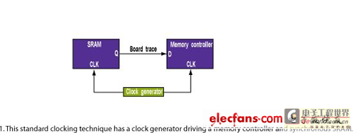
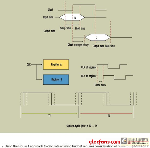
Figure 1 shows a standard timing system. In this figure, a memory controller is connected to an SRAM. Both the SRAM and the memory controller receive clock signals from the same clock source. Assuming that the clock signal circuit and circuit delay are intentionally matched here, the relevant timing parameters are as follows (Figure 2): memory controller tSU (setup time), memory controller tH (hold time), motherboard circuit tPD (transmission delay), SRAM tCO (clock to output delay), SRAM tDOH (output data hold time), clock generator tSKEW (clock skew), clock generator tJIT (cycle jitter), and clock generator tCYC (cycle time).
If the worst-case input setup time, clock-to-output delay, transmission delay, clock skew, and clock jitter are considered, the minimum cycle time of the system can be obtained by calculating the maximum frequency. The maximum frequency is calculated as follows:
tCO(max, SRAM) + tPD(max) + tSU(max, CTRL) + tSKEW(max, CLK) + tJIT(max, CLK) < tCYC
By calculating the hold time, it can be found that the system outputs data too quickly, affecting the input hold time of the system receiving device. In this way, the worst case will occur when the data is output earliest. The calculation formula is as follows:
tCO(min, SRAM) + tPD(min) - tSKEW(min, CLK) - tJIT(min, CLK) > tH(max, CTRL)
Now let's assume that the timing parameter values of the SRAM and memory controller are: tSU=0.5ns;tH=0.4ns;tCO=0.45ns;tDOH*=-0.45ns;tSKEW=±0.2ns;tJIT=±0.2ns. In this case, we will use a high-speed SRAM with a double data rate (DDR) interface, and the SRAM drives data on the rising and falling edges of each clock.
*tDOH < 0 means that the data becomes invalid before the next clock rising/falling edge. The required minimum hold time is calculated as follows:
tDOH + tPD - tSKEW - tJIT > tH
-0.45 ns + tPD - 0.2 ns - 0.2 ns > 0.4 ns
-0.85ns + tPD > 0.4ns
tPD > 1.25 ns
Assume that the propagation delay of the trace on the FR4 circuit board is 160ps/inch. The trace length from the SRAM to the memory controller is at least 7.82 inches. With tPD taken as 1.2ns, the maximum operating frequency can be calculated as follows. Because the SRAM has a DDR interface, the timing budget is based on half a clock cycle:
tCO + tPD + tSU + tSKEW + tJIT < tCYC/2
0.45ns+1.25ns+0.5ns+0.2ns+0.2ns
2.6ns
5.2ns
192MHz>fCYC
Under the premise of 7.82 inches of trace length on FR4 circuit board and typical timing parameters, the timing budget requirements can be met when the operating frequency is up to 192MHz. For systems with limited board space, the minimum trace length constraint of 7.82 inches becomes a requirement that is difficult for the system to meet.
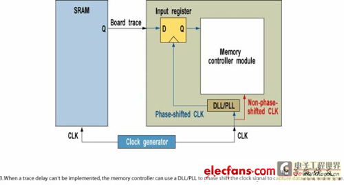
If adding routing delays is not an option, the memory controller can meet the hold time requirement by using a delay-locked loop/phase-locked loop (DLL/PLL) to phase-shift the clock signal to capture the data earlier (Figure 3). The memory controller will have to resynchronize the captured data with the system clock signal. Using this approach will introduce additional PLL/DLL jitter, which will reduce the maximum operating frequency of the system. With this additional PLL delay, the minimum required hold time becomes:
tDOH + tPD(trace) + tPLL/DLL_DELAY - tSKEW - tJIT > tH
tCO + tPD + tSU + tSKEW + tJIT + tJIT_PLL/DLL < tCYC/2
Where tJIT_PLL/DLL is the delay introduced by the PLL. Even with the fastest SRAM and ASIC/FPGA, clock skew, clock jitter, and circuit propagation delays can significantly limit system performance.
As mentioned earlier, if an FR4 board is used, the trace delay is about 160ps/inch. This number is very important given that the data valid window has become 2ns (for example, for 250MHz DDR devices) or even smaller at very high frequencies. The skew between clock signals will also significantly reduce the timing margin. We will see that source synchronous clocks can significantly reduce transmission delays, skew, and jitter, making timing closure easier to achieve.
Advantages of Source Synchronous Timing
In a typical source synchronous process, the rising edge of the clock associated with each data word is sent out (DDR memory may have multiple data per clock cycle), and the receiving device uses this rising edge of the clock to latch the data, and then synchronizes the data with the master clock or common clock. The same device synchronizes the clock signal and the data/control signal and transmits them, which actually eliminates the transmission delay of the motherboard circuit signal relative to the clock signal.
However, using source synchronous timing requires different motherboard routing considerations. In a system with a separate clock generator that provides clock signals to multiple devices, the first issue is to design the circuit length so that all clock edges arrive at the device at the same time, which may require extending the trace length connecting the device next to the clock generator.
With source synchronous methods, the main issue is to maintain phase alignment between the clock and data by matching the trace lengths of the output clock and data signals. If the traces are properly matched, data transmission delay relative to the clock signal no longer exists.
There are many ways to implement source synchronous timing:
1) The rising edge of the source synchronous clock signal is aligned to the start of the data valid window. Most DDR memories such as QDR-II/DDR-II SRAM use this method, where the memory sends both the clock signal and the data to the receiver. This article will use them as examples for discussion.
2) QDR-II generates a pair of output clock signals CQ and /CQ, ideally with a phase difference of 180° between them, and the receiver uses the rising edges of these two clock signals to latch data.
In both memories, the receiver must delay the clock signal to meet the setup and hold times required to capture the data. This delay can be achieved by on-chip delay blocks, using PLLs or DLLs at the receiving end, or by using on-board trace delays.
These two methods are favored in FPGA design because of their frequency transfer capabilities. To use the same design at a higher frequency, the FPGA code can be modified to change the delay introduced by the PLL/DLL. In addition, ASICs always run at a specific frequency, and ASICs usually choose the board trace delay method.
There are also some source synchronous clock implementations that delay their source synchronous clock signal at the source and align it in the center of the data valid window. In this case, the user can directly implement the source synchronous clock signal to latch the data at the receiver (assuming the traces between the clock and data are matched).
Effects of Jitter
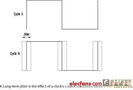
Jitter can be defined as the deviation of a clock bit transition from the ideal timing. The clock bit transition may be ahead or behind the ideal timing. There are several different types of jitter. Cycle-to-cycle jitter is the deviation of a clock output bit transition from the corresponding position in the previous cycle (see Figure 2). Period jitter measures the maximum deviation of a clock output bit transition from the ideal timing. Long-term jitter measures the maximum deviation of a clock output bit transition from the ideal timing over multiple cycles. The specific number of "multiple cycles" here depends on the specific application and operating frequency (Figure 4).
Depending on the application, one or all three types of jitter should be considered in the timing budget. In a synchronous timing environment, the clock source or PLL/DLL that generates the input clock generally causes jitter variation. When jitter is considered in the timing budget, jitter (tJIT) can significantly reduce timing margins, especially at high frequencies.
However, if the clock and data have the same jitter at the receiver, the jitter component (tJIT) can be removed from the timing budget. This is also true in the case of source synchronous clocking, where the clock signal and data are driven by the same transmitting device and remain aligned at all times. This effect is usually achieved when the clock is designed to be like one of the outputs. Although the clock-to-output time variation between the clock and data pins must still be considered, this parameter is generally around ±100ps.
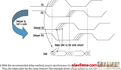
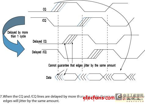
In some applications, the source synchronous clock is delayed by more than one cycle to latch the data. In this case, long-term jitter needs to be considered in the timing budget, which will reduce the timing margin. This jitter is also called N-cycle jitter, where N is the number of cycles that the source synchronous clock signal is delayed relative to the data signal. Of course, it is generally not recommended to delay the source synchronous clock signal by more than one cycle.
Timing Budget Calculation
As can be seen in the following examples, removing propagation delays from the timing budget can significantly improve system timing margins. Figure 5 shows an example of an SRAM using a source synchronous clock.

Let's calculate the timing budget as follows. By design, the rising edge of the SRAM output clock signal is aligned with the start edge of the data valid window. We assume that the memory controller delays the clock on-chip via PLL/DLL to meet the setup and hold times. The SRAM and memory controller use the same timing parameters.
Assuming that the clock and data trace lengths are matched, the circuit propagation delay tPD can be ignored when calculating the timing budget. In addition, the clock and data have the same skew and jitter (excluding the ±100 ps skew between pins), so there is no need to consider the clock generator jitter and skew (tSKEW, tJIT).
Another parameter to consider in this system is the SRAM's tJIT: the jitter of the SRAM output source synchronous clock relative to the data. This can be caused by variations in the clock-to-output time between pins.
In this example, we assume that the clock and data traces are well matched. If there is a difference in trace length due to circuit design, the difference in the trace length of the clock and data signals must be considered. If the trace of the clock signal is intentionally extended to delay the clock signal (align the clock signal with the center of the data valid window), this parameter does not need to be considered. Assuming the SRAM source synchronous clock jitter is tJIT=±0.2ns, we can calculate the minimum cycle time step by step as listed in the table (see table). To obtain a non-negative margin, the following conditions should be met:
tM>0
tCYC/2-2.2ns>0
tCYC/2>2.2ns
tCYC>4.4ns
fCYC<227MHz
This example uses a source synchronous clock signal to meet the setup and hold time requirements, and there is no constraint on the length of the data signal trace. The calculated maximum operating frequency is 277MHz, which is 35MHz higher than the traditional clock synchronization method. Note that the main frequency limiting factor in this example is the setup and hold time of the controller.
Best Practices for Using Source-Synchronous Clocks
To best utilize source synchronous clocking, designers should be aware of the following points:
Do not delay source-synchronous clocks by more than one cycle. The rising edge of a source-synchronous clock is closely matched to the data signal it drives, so the clock and data signals should have the same jitter and cancel each other out. If the rising edge of a source-synchronous clock signal is delayed until the next cycle to latch the data, then another jitter component must be considered, namely N-cycle jitter, where N is the number of cycles the clock signal is delayed relative to the data signal. Figures 6 and 7 show recommended and unrecommended methods for using source-synchronous clocks. These examples use QDR-II source-synchronous clocks (CQ and /CQ).
Note: If there are two source synchronous clocks, it is best to use both.
Previous article:High-voltage DAC powered from low-voltage supply generates tuning signal for filter
Next article:Problems and solutions of field bus control in thermal power plants
- High signal-to-noise ratio MEMS microphone drives artificial intelligence interaction
- Advantages of using a differential-to-single-ended RF amplifier in a transmit signal chain design
- ON Semiconductor CEO Appears at Munich Electronica Show and Launches Treo Platform
- ON Semiconductor Launches Industry-Leading Analog and Mixed-Signal Platform
- Analog Devices ADAQ7767-1 μModule DAQ Solution for Rapid Development of Precision Data Acquisition Systems Now Available at Mouser
- Domestic high-precision, high-speed ADC chips are on the rise
- Microcontrollers that combine Hi-Fi, intelligence and USB multi-channel features – ushering in a new era of digital audio
- Using capacitive PGA, Naxin Micro launches high-precision multi-channel 24/16-bit Δ-Σ ADC
- Fully Differential Amplifier Provides High Voltage, Low Noise Signals for Precision Data Acquisition Signal Chain
- Innolux's intelligent steer-by-wire solution makes cars smarter and safer
- 8051 MCU - Parity Check
- How to efficiently balance the sensitivity of tactile sensing interfaces
- What should I do if the servo motor shakes? What causes the servo motor to shake quickly?
- 【Brushless Motor】Analysis of three-phase BLDC motor and sharing of two popular development boards
- Midea Industrial Technology's subsidiaries Clou Electronics and Hekang New Energy jointly appeared at the Munich Battery Energy Storage Exhibition and Solar Energy Exhibition
- Guoxin Sichen | Application of ferroelectric memory PB85RS2MC in power battery management, with a capacity of 2M
- Analysis of common faults of frequency converter
- In a head-on competition with Qualcomm, what kind of cockpit products has Intel come up with?
- Dalian Rongke's all-vanadium liquid flow battery energy storage equipment industrialization project has entered the sprint stage before production
- New breakthrough! Ultra-fast memory accelerates Intel Xeon 6-core processors
- New breakthrough! Ultra-fast memory accelerates Intel Xeon 6-core processors
- Consolidating vRAN sites onto a single server helps operators reduce total cost of ownership
- Consolidating vRAN sites onto a single server helps operators reduce total cost of ownership
- Allegro MicroSystems Introduces Advanced Magnetic and Inductive Position Sensing Solutions at Electronica 2024
- Car key in the left hand, liveness detection radar in the right hand, UWB is imperative for cars!
- After a decade of rapid development, domestic CIS has entered the market
- Aegis Dagger Battery + Thor EM-i Super Hybrid, Geely New Energy has thrown out two "king bombs"
- A brief discussion on functional safety - fault, error, and failure
- In the smart car 2.0 cycle, these core industry chains are facing major opportunities!
- No GND vias + [Surface treatment]
- NUCLEO_G431RB Review (3) Oversampling 16-bit ADC
- ESP32 internal structure diagram
- SDIO connection to TF card initialization failed
- Servo Motor
- This Wednesday's award-winning live broadcast: 5G conformance testing and device acceptance testing
- Is it "reasonable..." to fly a kite made of your own photo?
- Battery Management System BMS Technical Data Transfer
- Beijing is urgently hiring FPGA development engineers, DSP development engineers, and hardware design engineers (fresh graduates are also welcome!)
- X-NUCLEO-IKS01A3 sensor test based on STM32F401RE development board 2 LPS22HH pressure sensor

 Digilent Vivado library
 W83116WG pdf Datasheet(V11 Low Power Clock Gen for Intel CK50


 京公网安备 11010802033920号