When we think of amplifiers that experience EOS problems, we probably think of electrostatic discharge (ESD). ESD subjects amplifier pins to a short, high-voltage, electrical discharge. A second (and often overlooked) overstress condition is EOS. EOS subjects amplifiers to lower overvoltages and currents than ESD, but for a longer period of time. After reading this article, you will have an understanding of potential amplifier EOS conditions and know how to address them. With this approach, you can design robust integrated circuit external systems that prevent electrical overstress damage. Destructive Electrostatic Discharge Events
An obvious cause of electrical overstress is ESD. ESD is possible when two bodies are in close proximity and at different electrostatic potentials (hundreds or thousands of volts). If a conductive path is created between the two bodies, static charge transfer occurs. Once the charge is neutralized, there is no further discharge. ESD can occur when the chip is out of circuit. Generally, we find that improper operation of IC chips can cause ESD, which can be destructive. ESD occurs within a fraction of a second (usually less than 250ns). If there is little resistance in the current path, a current of several amperes will flow into the chip circuit. Decades ago, semiconductor circuits often suffered from ESD damage, which eventually led to the failure of the entire circuit or even more harmful parameter degradation. However, once the characteristics of ESD were understood, semiconductor manufacturers began to implement protection circuits in new IC designs. These on-chip protection circuits greatly reduced the possibility of ESD damage to IC chips. The primary function of on-chip ESD protection circuitry is to prevent ESD-related damage from pre-PCB assembly and PCB assembly operations. During such operations, a low-impedance path to ground can act as a discharge path to discharge any charge carried by the IC or surrounding surfaces. Once the IC is mounted on the PC board, the situation is different. Once mounted, a connection is made between the IC chip and another on-board component. This greatly reduces the possibility of a low-impedance ESD path existing. After this installation, you will most likely not encounter ESD conditions that interfere with the internal ESD IC circuitry. That's good! However, there is another possibility. Some conditions in the operating circuitry can cause the IC chip to be affected by EOS. During the EOS condition, the ESD circuitry can be inadvertently activated. The time lag of the EOS can be much longer than the duration of the ESD. The intensity and duration of the current conducted during the EOS can be enough to generate dangerous levels of heat in the chip. Under such extreme conditions, the chip will be quickly damaged and inevitably, and the circuit will eventually be damaged. Phantom Electrical Overstress
Without realizing it, we may be relying on the device's internal ESD circuitry to provide protection during an EOS, even though the circuitry was not intended to support this purpose. You may find that you have an IC that works perfectly before power is applied (see Figure 1), but suddenly the IC is destroyed after power and input signals are applied. An EOS can be so severe that the IC overheats, melting the die and packaging materials. Figure 2 shows an example of this type of destruction.
Figure 1 Fully functional IC before installation
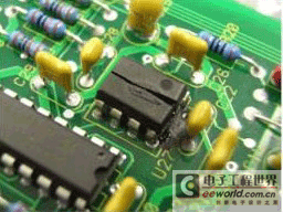
Figure 2: IC damaged after EOS Integrated circuits typically do not include protection for EOS conditions. At best, internal ESD protection circuits may be enabled during EOS and provide adequate protection. However, designing ESD protection circuits does not guarantee that this protection will be provided during all EOS conditions. The current paths established during EOS are complex and somewhat unpredictable, especially at high frequencies where stray impedances become large. Figure 3 shows several examples of possible current paths within the amplifier. The ESD input protection diodes (usually "off") provide a DC path to the various supplies and T1. If the amplifier supplies cannot sink the EOS-related currents, the IC supply pin voltages may rise to dangerous levels. T1 is an ESD absorption device. During ESD, the function of T1 is to turn on and clamp the voltage of the supply pins at a safe level. Remember that most ESD events occur when the IC is in a circuit disconnected state. However, during an in-circuit EOS, T1 may inadvertently turn on. In this case, T1 establishes a low resistance connection between the op amp supply pins. Thus, a strong destructive current begins to flow until T1 melts, creating a short circuit between the amplifier supplies. The self-heating and destruction mentioned earlier can occur. The heat can rise high enough to melt and crack the package, as shown in Figure 2.
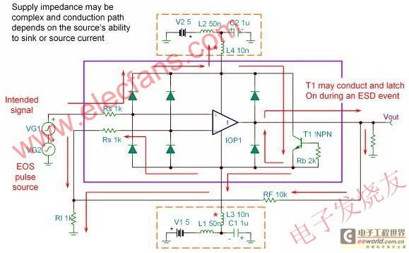
Figure 3 EOS activation multiple paths diagram translation:
(Upper left black) The source impedance can be complex and the conduction path will sink or source current depending on the source's ability
(Upper left) Target signal
(Lower left) EOS pulse source
(Top right) T1 may conduct and latch on during an ESD eventAs a major design consideration, it is important to ensure that all paths through the device can safely withstand the currents and voltages that occur during an EOS event. If you cannot anticipate these conditions and your IC cannot dissipate the heat generated, the circuit may be damaged. Understanding the internal ESD circuits of the amplifier and predicting how they will behave during an EOS event is an effective way to avoid these problems. Most op amp manufacturers can provide information on their ESD circuits. Example of EOS Conditions
Figure 4, generated using the TINA software tool and the OPA364 macro model, is an example of a simple follower circuit using the low-power OPA364 CMOS operational amplifier. The low-frequency signal VG1 represents the signal from the output of the transducer. The transducer is remote from the amplifier, and a cable (TL1) connects them. In this circuit, the surrounding environment causes transients to appear on the cable.
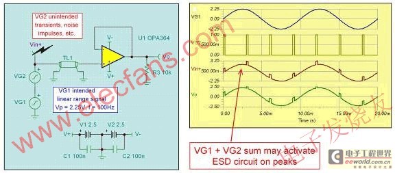
Figure 4 Input overdrive may activate ESD protection circuit diagram Translation:
(Top left) VG2 unintended transients, noise impulses, etc.
(Left figure below) VG1 intended linear range signal VP=2.25.f=100Hz
(right figure, bottom) VG1+VG2 sum may activate ESD circuit on peaks VG2 is an unintended transient signal combined with the transmitter output signal (VG1). The total signal amplitude exceeds the maximum specified input range of the amplifier. A sufficiently strong transient signal will trigger the op amp input ESD circuit. The resistor located in front of the non-inverting input of the amplifier limits the amount of input current generated. ESD cells are designed to safely conduct several amperes of current for very short periods of time, which does not exceed tens to hundreds of nanoseconds. When the ESD cell activates during an EOS event, the current conduction time depends on the EOS pulse or overvoltage characteristics. These same ESD cells can generally handle five to ten milliamps of current continuously, and the continuous current amperes can be greatly increased when the duty cycle is reduced. Under these conditions, they can be very safe and unaffected by overvoltage. In some applications, the input signal appears before the supply voltage is applied to the amplifier (see Figure 5). This plot was generated using the TINA software tool and the OPA374 macromodel. This power-up behavior has the potential to damage the input ESD protection circuitry if the current is not limited to a safe value.
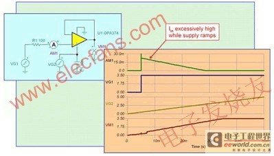
Figure 5 Watch Vin during power-up! Translation: (Top right) Iin excessively high while supply ramps In Figure 5, the supply (VG2) ramps from 0V to 5V in 50ms. This is accomplished by applying a 3.5V input signal (VG1) 5ms after the supply begins ramping. In this case, the input starts at a voltage above the positive rail. This turns on the non-inverting input ESD diode. Current flows out of the non-inverting input (AM1) until the voltage difference between the supply and input drops below about 0.6V. If the input source is low impedance and can provide current, there is little to no limit on it in the circuit. Under these conditions, a potentially damaging current flows through the ESD diode. Installing series input resistors protects the input circuit from this type of damage. The input (VG1) quickly reaches 3.5V during the amplifier transition time. On the other hand, the output (VM1) reaches the peak value of the input pulse when the amplifier is switching. During the amplifier switching time, the circuit creates a large input-output voltage difference. Initially, the difference between the input and the output is 10V. At the same time, the internal circuitry and feedback components of the op amp must handle the current flowing into the amplifier input (AM1) during this time. Another potentially damaging situation occurs when the amplifier input is subjected to a large signal, i.e., a fast edge pulse (see Figure 6). This figure was generated using the TINA software tool and the OPA277 macro model. In this case, the signal at VG1 applies a 10V peak rectangular pulse to the input. The amplifier responds to this pulse by generating a linear ramp output voltage. The finite slew rate of the amplifier (in this case, the OPA227 slew rate is equal to 2V/us) dictates the characteristics of the output voltage.
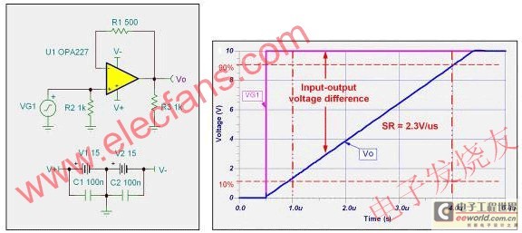
Figure 6 Input-to-Input Stress During Input Transitions (Top Right) Input-Output Voltage Difference During the transition times shown in Figure 6, there is a large input-to-output voltage difference during the time it takes the output to reach the peak value of the input pulse. Initially, the voltage difference between the amplifier input and output is 10V. This voltage difference decreases as the amplifier transitions to its final level. Since the inverting input initially has the same potential as the output, there is a 10V voltage difference between the two inputs. If the op amp does not include an internal input-to-input clamp, destructive voltage levels may be applied to the semiconductor junctions of the input transistors. This is a more serious problem with bipolar input op amps. Today's modern bipolar input op amps almost all include protection clamps. Some op amps exhibit an output reversal characteristic that is accompanied by an input overdrive (see Figure 7). This phenomenon is generally referred to as output phase reversal. Most modern op amps do not exhibit this phenomenon, but some op amps do exhibit it unexpectedly. For those op amps that have this characteristic, it generally occurs only when the applied input level exceeds the product's specified common-mode voltage (CMV) range. When an op amp exhibits output phase reversal, precautions must be taken to prevent the input from being overdriven.
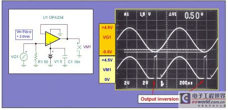
Figure 7 Output Inversion During Input Overdrive (Right) Output Inversion In Figure 7, the amplifier input (VG1) is driven to approximately 0.5V below the negative rail. The output level immediately switches from the negative rail to the positive rail. As the input is further overdriven, the output inversion lasts longer. Even though this may not damage the amplifier, it is a non-ideal condition that can have destructive consequences for the load if it is electromechanical in nature (i.e., motor, actuator, etc.). This overdrive problem can be solved by placing a small signal, reverse biased Schottky diode between the non-inverting input and the negative rail. A series input resistor should be included to limit the current through the diode. Switching power supply outputs can contain high frequency, transient energy. Even if filtering is included in these supplies, the voltage "spikes" at the output can still produce transient overvoltage conditions on the amplifier's supply pins. If the supply voltage exceeds the amplifier's voltage breakdown limit, the ESD absorption device may be triggered, forming a conduction path between the supply pins.
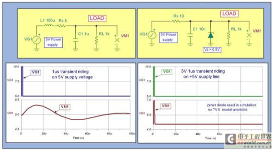
Figure 8 Power pin overvoltage protection diagram Translation:
(Left) 1us transient riding on 5V supply voltage
(Top right) 5V 1us transient riding on +5V supply line
(Bottom right) Zener diode used in simulation on TVS model available
A. Limits input current with RLC circuit
B. Limits input voltage with TVS Using RC or RLC circuits, you can protect devices from power supply transients (see Figure 8). A common on-board EMI/RFI filter will do the job. However, the response of the circuit varies greatly depending on the RLC constant and the load characteristics. In Figure 8A, a simple RLC circuit is connected to a load resistor. The +5V supply has a voltage of 5V, and a 1us transient equals a 10V voltage peak. This exceeds the maximum supply voltage of some low-voltage CMOS processes. The 1kΩ load resistor simulates an amplifier that requires about 5mA of supply current. From the response, you can see that the RLC circuit incorporates this peak into a sinusoidal response at the +5Vdc level. Slight overvoltages will not cause problems for the device. However, in many cases, some unknown conditions related to the combination of the RLC circuit can cause the power supply voltage to undershoot. This affects the output offset of the op amp. Although the PSRR of the op amp will help minimize changes in the output offset, it is also a significant error. Because too many variables are unknown, it is best not to rely on this type of protection. A better and more predictable method of transient suppression is to use a transient voltage suppressor (TVS) on the power supply line (see Figure 8B). A TVS is similar to a Zener diode, but is designed to withstand very large transient currents and peak powers. The TVR Littlefuse 1.5KE series is available in both unipolar and bipolar op amps with reverse withstand voltages from 6.8V to 550V. The peak power capability is 1500W for 10 100us pulses. They are some of the fastest responding devices with nanosecond response times. A clear advantage is the fast voltage clamping feature with minimal, if any, supply voltage undershoot. Figure 9 shows a complete EOS protection scheme using external protection devices. If you understand the internal ESD cells used on each op amp pin, some of the external devices can be eliminated as long as the internal devices can fully protect the individual op amp pins.
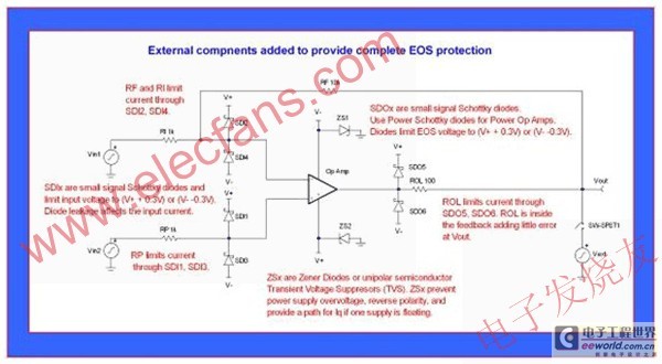
Figure 9 Complete external EOS protection diagram translation:
(title)
External components added to provide complete EOS protection
(Top left)
RF and RI limit current through SD12 and SD14
(Middle left)
SCOx are small signal schottky diodes and limit input voltage to (V. +0.3) or (V. -0.3). diode leakage affects the input current.
(Top right)
SCOx are small signal schottky diode. use power schottky diode for power OP amps. diode limit EOS voltage to(V. +0.3) or (V. -0.3)
(middle right)
ROL limits current through SDO5,SDO6. ROL is inside the feedback adding little error at Vcut. (Bottom center)
ZSx are zener diodes or input semiconductor transient voltage suppressors (TVS). ZSx prevent power supply overvoltage. Reverse polarity, and provide a path for lq if one supply is floating.SDIx Schottky diodes provide voltage clamping for input overvoltage. R1 limits the current through these diodes to the specified level for the diodes used. SDOx Schottky diodes provide voltage clamping for output overvoltage. If you use this output protection on the op amp power supply, use power Schottky diodes. The current through these diodes must be limited to the specified level for the diodes used. Once you allow this transient current to flow through the input or output diodes, you must drain this energy to ground or the op amp power supply may go into an overvoltage condition. If this happens, the amplifier will latch up or even be permanently damaged. If the power supply cannot sink current, or has a low impedance at the non-diode DC current frequency, then a Zener diode or DC voltage suppressor (TVS) is required on each supply to direct this current to ground. Most power supplies are unidirectional, not bidirectional, sourcing or sinking current. Zener diodes or unidirectional semiconductor transient voltage suppressors provide a simple, low-cost method of maintaining device pins at safe levels. Conclusion
An EOS event may activate the ESD protection circuitry in the op amp. You might be tempted to think that the ESD circuitry is also well suited to handle EOS events. ESD events are very short, typically less than a few hundred nanoseconds. In contrast, EOS events can last much longer. When the ESD circuitry is activated by an EOS event, the circuitry conducts current that may cause overheating, which may result in some damage. If your system is faced with an EOS event, use a simple external protection circuit to protect your circuitry. This can save you from some back-end design headaches, albeit with some minor front-end design issues.
Previous article:Circuit Design and Simulation of Ultra-Wideband (UWB) Receiver
Next article:SDL-109A-T1 Signal Interruption Amplifier Parameter Introduction
Recommended ReadingLatest update time:2024-11-16 22:27


- Popular Resources
- Popular amplifiers
-
 Operational Amplifier Practical Reference Handbook (Edited by Liu Changsheng, Zhao Mingying, Liu Xu, etc.)
 -
 A Complete Illustrated Guide to Operational Amplifier Applications (Written by Wang Zhenhong)
 -
 Design of isolated error amplifier chip for switching power supply_Zhang Rui
 -
 DAM medium wave transmitter high frequency power amplifier module test platform_Tian Tian
- High signal-to-noise ratio MEMS microphone drives artificial intelligence interaction
- Advantages of using a differential-to-single-ended RF amplifier in a transmit signal chain design
- ON Semiconductor CEO Appears at Munich Electronica Show and Launches Treo Platform
- ON Semiconductor Launches Industry-Leading Analog and Mixed-Signal Platform
- Analog Devices ADAQ7767-1 μModule DAQ Solution for Rapid Development of Precision Data Acquisition Systems Now Available at Mouser
- Domestic high-precision, high-speed ADC chips are on the rise
- Microcontrollers that combine Hi-Fi, intelligence and USB multi-channel features – ushering in a new era of digital audio
- Using capacitive PGA, Naxin Micro launches high-precision multi-channel 24/16-bit Δ-Σ ADC
- Fully Differential Amplifier Provides High Voltage, Low Noise Signals for Precision Data Acquisition Signal Chain
- Innolux's intelligent steer-by-wire solution makes cars smarter and safer
- 8051 MCU - Parity Check
- How to efficiently balance the sensitivity of tactile sensing interfaces
- What should I do if the servo motor shakes? What causes the servo motor to shake quickly?
- 【Brushless Motor】Analysis of three-phase BLDC motor and sharing of two popular development boards
- Midea Industrial Technology's subsidiaries Clou Electronics and Hekang New Energy jointly appeared at the Munich Battery Energy Storage Exhibition and Solar Energy Exhibition
- Guoxin Sichen | Application of ferroelectric memory PB85RS2MC in power battery management, with a capacity of 2M
- Analysis of common faults of frequency converter
- In a head-on competition with Qualcomm, what kind of cockpit products has Intel come up with?
- Dalian Rongke's all-vanadium liquid flow battery energy storage equipment industrialization project has entered the sprint stage before production
- Allegro MicroSystems Introduces Advanced Magnetic and Inductive Position Sensing Solutions at Electronica 2024
- Car key in the left hand, liveness detection radar in the right hand, UWB is imperative for cars!
- After a decade of rapid development, domestic CIS has entered the market
- Aegis Dagger Battery + Thor EM-i Super Hybrid, Geely New Energy has thrown out two "king bombs"
- A brief discussion on functional safety - fault, error, and failure
- In the smart car 2.0 cycle, these core industry chains are facing major opportunities!
- The United States and Japan are developing new batteries. CATL faces challenges? How should China's new energy battery industry respond?
- Murata launches high-precision 6-axis inertial sensor for automobiles
- Ford patents pre-charge alarm to help save costs and respond to emergencies
- New real-time microcontroller system from Texas Instruments enables smarter processing in automotive and industrial applications
- COVID-19 and other challenges to LED design and coping strategies
- purchase
- Shocked! One person made a company popular
- [Liquid Level Sensor Evaluation] A/D Data Acquisition and Numerical Display
- [Evaluation of EC-01F-Kit, the NB-IoT development board of Anxinke] + Try to connect the serial port assistant to Alibaba Cloud
- [Jihai APM32E103VET6S MINI Development Board Review] Part 4: Key Interrupt
- Technology Popularization: Do you know why base stations are painted in colors?
- Usage of ^ in Verilog
- A brief list of long and short distance wireless communication technologies
- A classic foreign book about semaphores

 Operational Amplifier Practical Reference Handbook (Edited by Liu Changsheng, Zhao Mingying, Liu Xu, etc.)


 京公网安备 11010802033920号