introduction
ADC is the bridge connecting the analog signal processing part and the digital signal processing part in modern digital demodulators and software radio receivers. Its performance determines the overall performance of the receiver to a large extent. There are many sources of noise introduced during the A/D conversion process, mainly including thermal noise, ripple of the ADC power supply, ripple of the reference level, phase noise caused by sampling clock jitter, and noise caused by quantization errors. In addition to the inevitable noise introduced by quantization errors, many measures can be taken to reduce the noise power before reaching the ADC, such as using an amplifier with better noise performance, reasonable circuit layout, reasonable design of the sampling clock generation circuit, and reasonable design of the ADC. Power supply and use of decoupling capacitors, etc. This article mainly discusses the impact of sampling clock jitter on ADC signal-to-noise ratio performance and the design of low-jitter sampling clock circuits.

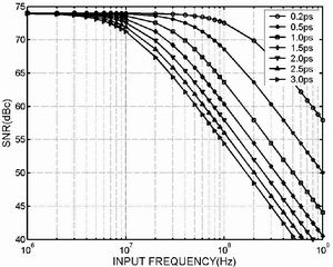
(a) Ideal signal-to-noise ratio of 12-bit ADC

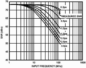
(b) Measured signal-to-noise ratio of AD9245
Figure 1 Schematic diagram of the signal-to-noise ratio of the 12-bit ADC under different clock jitter conditions
Clock jitter on ADC
Effect of signal-to-noise ratio
The jitter of the sampling clock is a short-term, non-cumulative variable that represents the time deviation between the actual timing position of a digital signal and its ideal position. The jitter generated by the clock source will cause the internal circuit of the ADC to trigger the sampling time incorrectly, resulting in missampling of the amplitude of the analog input signal, thereby deteriorating the signal-to-noise ratio of the ADC.
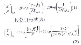
When the clock jitter is given, the maximum signal-to-noise ratio of the ADC can be calculated using the following formula:

According to formula (2), Figure 1 shows the ideal signal-to-noise ratio and the measured signal-to-noise ratio of the ADC under different clock jitter conditions when the number of quantization bits is 12-bit.
It can be seen from Figure 1 that the jitter of the clock has a very obvious impact on the deterioration of the signal-to-noise ratio performance of the ADC. The higher the frequency of the signal entering the ADC under the same jitter condition, the greater the deterioration of its performance. For the same input signal frequency, Under this circumstance, the greater the jitter of the sampling clock, the greater the deterioration of the ADC signal-to-noise ratio performance. Comparing the two schematic diagrams in Figure 1, we can see that the measured impact of sampling clock jitter on the ADC signal-to-noise ratio performance is very consistent with the results obtained from the theoretical analysis, which also proves the correctness of the theoretical analysis. Therefore, in actual applications, the A/D conversion chip cannot be selected entirely based on the ideal signal-to-noise ratio formula. Instead, one should refer to the measured performance curve given by the chip manufacturer and the jitter performance of the designed sampling clock to reasonably select the one that suits the design needs. A/D conversion chip, and leave a certain design margin.

Figure 2 A practical low-jitter clock generation circuit
Two practical low-jitter sampling clock generation circuit
clock jitter generation mechanisms
It is difficult to directly measure clock jitter, and indirect measurement methods are generally used. For this reason, this section first gives the generation mechanism of clock jitter. Clock jitter is caused by various noise sources inside the clock generation circuit (usually a phase-locked loop based on a low-phase noise voltage-controlled oscillator), such as thermal noise (mainly the thermal noise floor of the voltage-controlled oscillator output signal) , phase noise and spurious noise, etc. Theoretical analysis shows that when the required frequency is higher, the deterioration of clock jitter by phase noise and spurious noise is not obvious.
Generally speaking, the thermal noise floor of the VCO output stage amplifier can be regarded as Gaussian white noise with a limited bandwidth, and its effective bandwidth is approximately twice the operating frequency. When the VCO is correctly tuned to the desired output frequency, the effect of the noise floor on jitter can be calculated using the following formula:

In the formula, f0 is the center frequency of the oscillator, f represents the offset relative to the center frequency, and L(f) is the phase noise at the frequency offset f (unit is dBc/Hz). In order to further improve the performance of the system, people often use a power matching network with a frequency response similar to a band-pass filter at the output end of the VCO, which has a certain attenuation effect on noise outside the bandwidth. In this way, the worst-case noise can be estimated using the integral from 0 Hz to f0. The noise outside this range is greatly attenuated and can be ignored, because the noise floor from 0 to f0 is smooth, L( f) can be regarded as a constant, so formula (3) is simplified to:

Therefore, the edge clock jitter caused by the noise floor is:

Theoretically, it can be considered that the phase noise characteristics of the output signal from the phase-locked loop are basically the same as those of the VCO. However, the actual phase-locked circuit will introduce a certain amount of noise, and the VCO output amplifier will also worsen the phase noise characteristics of the generated clock signal. . Therefore, when designing a phase-locked loop circuit, in addition to choosing a VCO with lower phase noise, you should also choose an amplifier or clock buffer with a lower noise figure, and try to separate the clock generation circuit from other circuits. .
Variable sampling clock based on low phase noise VCO
Figure 2 shows a practical low-jitter variable sampling clock generation circuit based on a low-phase noise VCO.
In Figure 2, MC145170 is used as the frequency synthesizer for the clock generation loop, and Mini-Circuits company's low phase noise voltage controlled oscillator POS-200 is selected as the frequency synthesizer.

If the ADC used is AD9245, it can be seen from Figure 1: When the ADC front-end input signal frequency is lower than 50MHz, the signal-to-noise ratio of AD9245 will be better than 65dB. When the input signal frequency is lower than 100MHz, the signal-to-noise ratio of AD9245 will be better than at 60dB.
Non-variable sampling clock based on extremely low phase noise temperature compensated crystal oscillator
After determining the sampling frequency, if the clock generated by the clock generation circuit is not required to be variable, a clock generation method based on a temperature-compensated crystal oscillator can be used. First, the maximum allowable clock jitter is determined based on the required ADC signal-to-noise ratio by formula (2), and then the maximum tolerated phase noise floor is deduced from formula (5). Finally, the phase noise characteristics at different frequency deviation points are given and intersected. It can be customized by the crystal oscillator manufacturing factory. This is the simplest time generation method, which basically does not require much debugging, but it is only suitable for fixed clock sampling.
When using the above two methods to generate a sampling clock, one thing worth noting is that the sampling clock circuit should be as independent as possible from the digital system with noise, and there should be no logic gate circuits in the path of the sampling clock. Generally speaking, , a logic gate will produce timing jitter of several picoseconds or even more than ten picoseconds. The sampling clock generation circuit should be separated from the digital and analog parts of the system during design.
Conclusion
This article first analyzes the impact of sampling clock jitter on ADC signal-to-noise ratio performance, then points out the reasons for the generation of time jitter, and finally gives two practical sampling clock generation solutions: a variable sampling clock based on low phase noise VCO and a variable sampling clock based on Method for generating a non-variable sampling clock from an extremely low phase noise temperature compensated crystal oscillator.
references
1 James Tsui.Translated by Yang Xiaoniu and others. Broadband digital receiver[M]. Beijing: Electronic Industry Press, 2002
2 AD9245 Datasheet.Analog Devices, Inc. 2003
3 Steve Lee, Ken Yang.Design a Low-Jitter Clock for High-Speed Data Converters[J].Maxim application note, 2001
4 Yang Xiaoniu, Lou Caiyi, Xu Jianliang. Principles and applications of software radio[M]. Beijing: Electronic Industry Press, 2001
5 Peng Fei. Research and implementation of bandpass sampling and digital down-conversion[D]. School of Communication Engineering, PLA University of Science and Technology, 2004
Previous article:Application of digital potentiometer
Next article:10 factors that must be considered when working together with DSP and data converters
- High signal-to-noise ratio MEMS microphone drives artificial intelligence interaction
- Advantages of using a differential-to-single-ended RF amplifier in a transmit signal chain design
- ON Semiconductor CEO Appears at Munich Electronica Show and Launches Treo Platform
- ON Semiconductor Launches Industry-Leading Analog and Mixed-Signal Platform
- Analog Devices ADAQ7767-1 μModule DAQ Solution for Rapid Development of Precision Data Acquisition Systems Now Available at Mouser
- Domestic high-precision, high-speed ADC chips are on the rise
- Microcontrollers that combine Hi-Fi, intelligence and USB multi-channel features – ushering in a new era of digital audio
- Using capacitive PGA, Naxin Micro launches high-precision multi-channel 24/16-bit Δ-Σ ADC
- Fully Differential Amplifier Provides High Voltage, Low Noise Signals for Precision Data Acquisition Signal Chain
- Innolux's intelligent steer-by-wire solution makes cars smarter and safer
- 8051 MCU - Parity Check
- How to efficiently balance the sensitivity of tactile sensing interfaces
- What should I do if the servo motor shakes? What causes the servo motor to shake quickly?
- 【Brushless Motor】Analysis of three-phase BLDC motor and sharing of two popular development boards
- Midea Industrial Technology's subsidiaries Clou Electronics and Hekang New Energy jointly appeared at the Munich Battery Energy Storage Exhibition and Solar Energy Exhibition
- Guoxin Sichen | Application of ferroelectric memory PB85RS2MC in power battery management, with a capacity of 2M
- Analysis of common faults of frequency converter
- In a head-on competition with Qualcomm, what kind of cockpit products has Intel come up with?
- Dalian Rongke's all-vanadium liquid flow battery energy storage equipment industrialization project has entered the sprint stage before production
- Allegro MicroSystems Introduces Advanced Magnetic and Inductive Position Sensing Solutions at Electronica 2024
- Car key in the left hand, liveness detection radar in the right hand, UWB is imperative for cars!
- After a decade of rapid development, domestic CIS has entered the market
- Aegis Dagger Battery + Thor EM-i Super Hybrid, Geely New Energy has thrown out two "king bombs"
- A brief discussion on functional safety - fault, error, and failure
- In the smart car 2.0 cycle, these core industry chains are facing major opportunities!
- The United States and Japan are developing new batteries. CATL faces challenges? How should China's new energy battery industry respond?
- Murata launches high-precision 6-axis inertial sensor for automobiles
- Ford patents pre-charge alarm to help save costs and respond to emergencies
- New real-time microcontroller system from Texas Instruments enables smarter processing in automotive and industrial applications
- USB Type-C interface desktop monitor dedicated solution - single interface solution
- How is this switching transformer wound?
- How to delete products on Pingtouge's scenario-based Bluetooth Mesh cloud platform
- [Sipeed LicheeRV 86 Panel Review] IV. Failure to compile system image: Struggle and clear direction
- He works overtime, so I work too. I can't run away even if I want to. Have you ever seen such an overtime slogan?
- F28335 PWM trigger ADC sampling code + comments
- 【TouchGFX Design】Installation and simple experience
- How is the output V0 of this op amp derived?
- How to configure AFE940? Does anyone have the documentation?
- The LCD screen uses the ILI9325 screen controller, and the 32-bit board is STM32F103ZET6. After burning the program, only the background is lit,...

 Building real-time machine learning systems
 Digilent Vivado library


 京公网安备 11010802033920号