A/D Converter Testing Techniques and Finding Missing Codes in ADCs
The quantization noise, dropped bits, harmonic distortion, and other nonlinear distortion characteristics of an A/D converter can be determined by analyzing the spectral components of the converter output.
It is not difficult to determine the degradation of converter performance caused by the above nonlinear characteristics, because these are manifested as some spurious spectral components in the output noise of the A/D converter and the increase of background noise. The traditional measurement method is to add an analog sinusoidal voltage to the input of the A/D converter and then measure the spectrum of the converter's digitized time domain output samples.
FFT can be used to calculate the spectrum of the A/D converter output samples, but in order to improve the sensitivity of the spectrum measurement, the FFT spectrum leakage must be minimized. However, for high-performance A/D converter testing, traditional time domain windowing cannot sufficiently reduce FFT leakage.
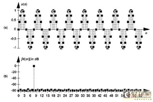
The trick to solving FFT leakage is to use an analog sinusoidal input voltage with a frequency that is an integer multiple of the A/D converter clock frequency, as shown in Figure 1(a). This frequency is mfs/N, where m is an integer, fs is the clock frequency (sampling rate), and N is the number of FFT points. When the analog input to an ideal A/D converter is an 8-cycle sampled sine wave from the N = 128 converter output, x(n) in Figure 1(a) is its time domain output.

Figure 1: When the input is a simulated 8fs/128 Hz sinusoid, the analog input to an ideal A/D converter is: (a) output time domain samples; (b) amplitude in dB.
In this example, the input frequency is normalized to the sampling rate fs, which is 8fs/128 Hz. mfs/N defines the analysis frequency, or bin center, of the discrete Fourier transform (DFT). A DFT input sinusoid with a frequency at the bin center will not cause spectral leakage.
In Figure 1(b), the first half of the 128-point FFT of x(n) is plotted on a logarithmic scale. The input frequency is exactly in the center of the frequency bin m = 8, and FFT leakage is effectively reduced. In particular, if the sampling rate is 1 MHz, the analog input frequency to the A/D must be exactly 8(106/128) = 62.5 kHz.
To achieve this, it is necessary to ensure that the analog test signal source is precisely synchronized with the A/D converter clock frequency fs Hz. This is why the A/D converter test process is called coherent sampling.
That is, the analog signal generator and the A/D clock generator that provides fs cannot drift in frequency with respect to each other and must remain coherent (note that from a semantic point of view, quadrature sampling is sometimes referred to as coherent sampling, but quadrature sampling has nothing to do with the A/D converter test process here).
As expected, some values of m are more favorable than others. Note in Figure 1(a) that when m=8, the A/D converter outputs only 9 different amplitude values. These values repeat over and over again. As shown in Figure 2 above, when n=7, there are many more than 9 different A/D output values.

Figure 2: 7-cycle sinusoidal A/D converter output.
Choose m to be an odd prime number
Since it is best to test as many A/D output binary words as possible while keeping the quantization noise sufficiently random, users of the A/D test solution discovered another trick. They found that the repetition of the A/D output words can be minimized when m is chosen to be an odd prime number (3, 5, 7, 11).
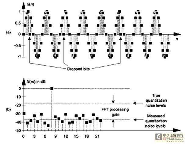
Figure 3(a) below shows an extreme example of a nonlinear A/D converter operation, with several discrete outputs dropping the sampled bits into the time domain x(n) with m = 8. Figure 3(b) provides the FFT of this distorted x(n), and when compared to Figure 1(b), it can be seen that the noise floor has increased, due to the nonlinearity of the A/D converter.

Figure 3: Non-ideal A/D converter output showing several missing bits: (a) time samples; (b) spectral amplitude (in dB).
The quantization noise level of a real A/D converter should be higher than the result measured in Figure 3(b) above. This is because the FFT-related processing gain raises the high-level m=8 spectral component in the background noise.
Therefore, if this A/D test technique is used, the FFT processing gain of 10log10(N/2) shown in Figure 3(b) must be calculated.
In order to fully characterize the dynamic performance of the A/D converter, this test needs to be performed at many different frequencies and amplitudes. Of course, the analog sinusoidal signal applied to the A/D converter must be as pure as possible. Any inherent distortion in the analog signal will show up in the final FFT output and cause A/D nonlinearity problems.
The key is that any input frequency must be mfs/N. Here m is less than N/2 in order to meet the Nyquist sampling criterion, fully utilizing the processing power of the FFT while minimizing frequency leakage.
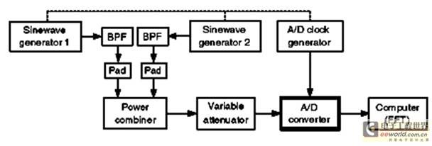
To quantify the intermodulation distortion of a converter, two analog signals are usually added to the input of the A/D. The intermodulation distortion in turn characterizes the dynamic range of the converter. In this case, both input signals must meet the mfs/N limit. The test configuration is shown in Figure 4.

Figure 4: A/D converter hardware test configuration.
When using a low-pass filter (BPF) to improve the purity of the output signal of a sine wave source, caution should be exercised and fixed attenuators (pads) with small attenuation should be used to prevent the two signal sources from interfering with each other. (A 3-dB attenuator is recommended).
A power combiner is usually the reverse application of an analog power divider, and the output of the A/D clock signal generator is also a square wave. The dotted line in Figure 4 above shows that all three signal sources are locked to the same reference frequency source.
Detecting missing code
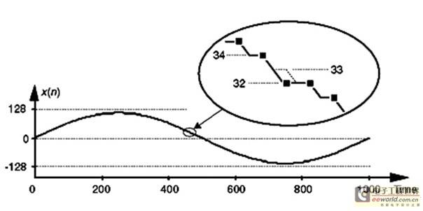
One problem that affects A/D converters is missing codes. This problem occurs when the converter fails to output a specific binary word (a code). Imagine driving an 8-bit converter with an analog sine wave. The output binary word should be 00100001 (decimal 33), but the actual output is 00100000 (decimal 32), as shown in Figure 5.

Figure 5: Time domain plot of the missing codes of binary 0010001, decimal 33, for an 8-bit converter.
The binary word representing decimal 33 is a missing code. This tiny nonlinearity is difficult to detect by testing time domain sampling or performing spectrum analysis. Fortunately, there is a simple and reliable way to detect the missing code using histogram analysis.
The statistical histogram analysis test technique simply involves collecting many A/D converter output samples and plotting the number of occurrences of these samples versus their values.
In this statistical histogram, any missing code (such as the missing 33 above) will be displayed as a zero value. In other words, the probability of this binary code representing decimal 33 appearing is zero.
Previous article:Using clock margining techniques to achieve system boundary stability and early failure
Next article:Beyond “Derating”: Reliability Concepts Worthy of Reference for Modern Engineers
Recommended ReadingLatest update time:2024-11-16 19:31


- Popular Resources
- Popular amplifiers
-
 Virtualization Technology Practice Guide - High-efficiency and low-cost solutions for small and medium-sized enterprises (Wang Chunhai)
 -
 A Complete Illustrated Guide to Operational Amplifier Applications (Written by Wang Zhenhong)
 -
 ESP32-S3 source code
 -
 【Follow me Season 2 Episode 2】Arduion UR4 homework submission code
- High signal-to-noise ratio MEMS microphone drives artificial intelligence interaction
- Advantages of using a differential-to-single-ended RF amplifier in a transmit signal chain design
- ON Semiconductor CEO Appears at Munich Electronica Show and Launches Treo Platform
- ON Semiconductor Launches Industry-Leading Analog and Mixed-Signal Platform
- Analog Devices ADAQ7767-1 μModule DAQ Solution for Rapid Development of Precision Data Acquisition Systems Now Available at Mouser
- Domestic high-precision, high-speed ADC chips are on the rise
- Microcontrollers that combine Hi-Fi, intelligence and USB multi-channel features – ushering in a new era of digital audio
- Using capacitive PGA, Naxin Micro launches high-precision multi-channel 24/16-bit Δ-Σ ADC
- Fully Differential Amplifier Provides High Voltage, Low Noise Signals for Precision Data Acquisition Signal Chain
- Innolux's intelligent steer-by-wire solution makes cars smarter and safer
- 8051 MCU - Parity Check
- How to efficiently balance the sensitivity of tactile sensing interfaces
- What should I do if the servo motor shakes? What causes the servo motor to shake quickly?
- 【Brushless Motor】Analysis of three-phase BLDC motor and sharing of two popular development boards
- Midea Industrial Technology's subsidiaries Clou Electronics and Hekang New Energy jointly appeared at the Munich Battery Energy Storage Exhibition and Solar Energy Exhibition
- Guoxin Sichen | Application of ferroelectric memory PB85RS2MC in power battery management, with a capacity of 2M
- Analysis of common faults of frequency converter
- In a head-on competition with Qualcomm, what kind of cockpit products has Intel come up with?
- Dalian Rongke's all-vanadium liquid flow battery energy storage equipment industrialization project has entered the sprint stage before production
- Allegro MicroSystems Introduces Advanced Magnetic and Inductive Position Sensing Solutions at Electronica 2024
- Car key in the left hand, liveness detection radar in the right hand, UWB is imperative for cars!
- After a decade of rapid development, domestic CIS has entered the market
- Aegis Dagger Battery + Thor EM-i Super Hybrid, Geely New Energy has thrown out two "king bombs"
- A brief discussion on functional safety - fault, error, and failure
- In the smart car 2.0 cycle, these core industry chains are facing major opportunities!
- The United States and Japan are developing new batteries. CATL faces challenges? How should China's new energy battery industry respond?
- Murata launches high-precision 6-axis inertial sensor for automobiles
- Ford patents pre-charge alarm to help save costs and respond to emergencies
- New real-time microcontroller system from Texas Instruments enables smarter processing in automotive and industrial applications
- STMicroelectronics launches the second generation multi-zone time-of-flight sensor VL53L8
- EEWORLD University - Wildfire FreeRTOS Kernel Implementation and Application Development Practical Guide
- Teach you how to make a lithium battery fast charging charger
- Solution to the problem of not being able to generate electrical connection network using Harness in Altium Designer
- 【ufun learning】02 Concept and preliminary circuit design 1
- 【RT-Thread Reading Notes】Reflections on RT-Thread Chapters 7-8
- DC-DC chip LM2596SX-5.0/NOPB
- How does the lwip client let the server know that it has been shut down?
- Small car front-end 16W power supply design
- Bear Pie Huawei IoT operating system LiteOS bare metal driver transplantation 05-E53_SF1 expansion board driver and use

 Virtualization Technology Practice Guide - High-efficiency and low-cost solutions for small and medium-sized enterprises (Wang Chunhai)
 ESP32-S3 source code
 【Follow me Season 2 Episode 2】Arduion UR4 homework submission code


 京公网安备 11010802033920号