74HC595 is one of the commonly used chips in the single-chip microcomputer system, just like 74hc164. Its function is to convert serial signals into parallel signals. It is commonly used in various digital tubes and dot matrix screen driver chips. Using 74HC595 can save the IO port resources of the single-chip microcomputer MCU. 3 IOs can control the pins of 8 digital tubes. It also has a certain driving ability and can avoid the amplifier circuits such as triodes. Therefore, this chip is a magic tool for driving digital tubes. It is widely used. Click here to download the complete 74HC595 Chinese information: http://www.51hei.com/f/74HC595中文资料.pdf
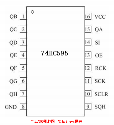
74HC595 Pin Diagram
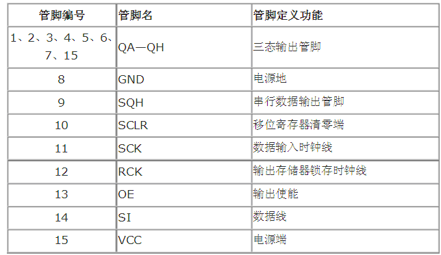
74HC595 Pin Function
Next, I will introduce the working principle of 74HC595:
Data terminal of 74HC595:
QA--QH: 8-bit parallel output terminal, which can directly control the 8 segments of the digital tube.
QH': Cascade output terminal. I will connect it to the SI terminal of the next 595.
SI: Serial data input terminal.
74hc595 control terminal description:
/SCLR (pin 10): When low, the data in the shift register is cleared. Usually I connect it to Vcc.
SCK (pin 11): Data shifts in the data register on the rising edge. QA-->QB-->QC-->...-->QH; the data in the shift register remains unchanged on the falling edge. (Pulse width: at 5V, it only needs to be greater than a few tens of nanoseconds. I usually choose microseconds)
Control shift register
SCK rising edge data shift SCK falling edge data hold
RCK (pin 12): The data of the shift register enters the storage register at the rising edge, and the data of the storage register remains unchanged at the falling edge. I usually set RCK to a low level. When the shift is completed, a positive pulse (at 5V, more than a few tens of nanoseconds is enough. I usually choose microseconds) is generated at the RCK end to update the displayed data.
Control storage register
The data of the shift register enters the storage register at the rising edge of RCK. The data of the storage register remains unchanged at the falling edge of RCK.
/G (pin 13): Disable output when high level (high impedance state). If the pins of the microcontroller are not tight, you can easily produce flashing and extinguishing effects by controlling it with one pin. It saves time and effort than controlling by shifting the data terminal.
Note: 74164 and 74595 have similar functions, both are 8-bit serial input to parallel output shift registers. The drive current of 74164 (25mA) is smaller than that of 74595 (35mA), and it has 14-pin package and smaller size.
The main advantage of 74595 is that it has a data storage register, and the data at the output end can remain unchanged during the shift process. This is very useful in situations where the serial speed is slow and the digital tube does not flicker.
Compared with 74hc164 which only has a data reset terminal, 74hc595 also has an output enable/disable control terminal oe, which can make the output high impedance. So it is more convenient to use this chip
74HC595 is an 8-bit shift register and a memory with three-state output function. The shift register and memory are clocked separately. Data is input on the rising edge of SHcp (see timing diagram) and goes to the storage register on the rising edge of STcp (see timing diagram). If the two clocks are connected together, the shift
The shift register is always one pulse ahead of the storage register. The shift register has a serial shift input (Ds), and a serial output
(Q7'), and an asynchronous low reset, the storage register has a parallel 8-bit bus output with three-state.
When OE is enabled (low level), the data in the storage register is output to the bus.
Here is the method of driving 74hc595 with a single-chip microcomputer: http://www.51hei.com/chip/1799.html
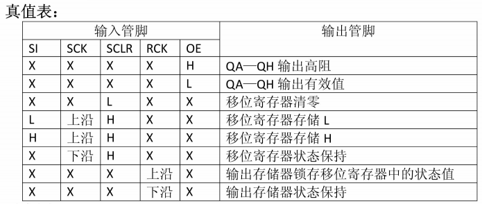
74HC595 Truth Table

74hc595 maximum and minimum voltage
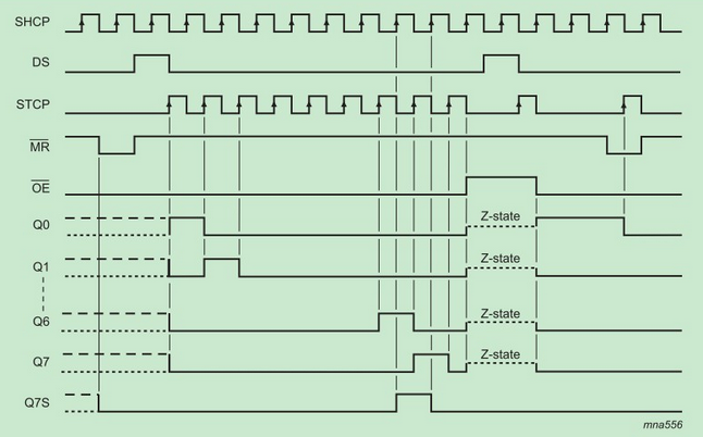
74HC595 Timing Diagram 74HC595 Logic Diagram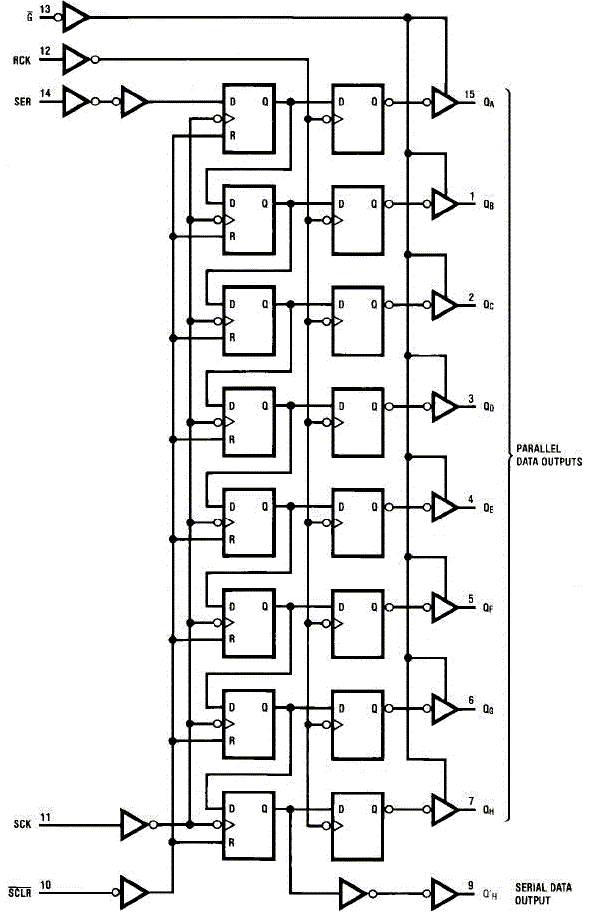
The main differences between 74HC595 and 74HC164 are:
1. The 74HC595 has a latch, so the output can remain unchanged during the shift process; while the 74HC164 does not have a latch, so the output changes once each shift clock is generated. This is the biggest difference between the two
2. 74HC595 uses the dedicated Q7' pin to achieve multi-chip cascading; 74HC164 directly uses the output pin Q7 cascade
3. 74HC595 has enable OE. When OE is invalid, the output pin is in high impedance state; while 74HC164 has no enable pin
4. The reset of 74HC595 is for the shift register. To reset the LATCH register, the ST_CP rising edge must be used to load the shift register content into the latch register. In other words, the reset of 74HC595 is synchronous, while the reset of 74HC164 is asynchronous, so the reset of 74HC164 is simpler.
5. 74HC164 has a corresponding 74HC165 parallel-to-serial chip
74HC595.c
-------------------------------------------------- -------------------------------------------------- --------------------------------------------------
#include "stm32f10x.h"
#include "stm32f10x_rcc.h"
#include "stm32f10x_gpio.h"
#include "74HC595.h"
/* Delay module 82615468 sp-320-12
* */
static void delay(u32 t)
{
u32 i;
while(t--)
for (i = 0; i < 1; i++);
}
void HC595Init(void)
{
GPIO_InitTypeDef GPIO_InitStructure;
RCC_APB2PeriphClockCmd(HC595_CLK_GPIO_CLK | HC595_DATA_GPIO_CLK | HC595_CS_GPIO_CLK, ENABLE);
GPIO_InitStructure.GPIO_Pin = HC595_CLK_PIN;
GPIO_InitStructure.GPIO_Speed = GPIO_Speed_2MHz;
GPIO_InitStructure.GPIO_Mode = GPIO_Mode_Out_PP;
GPIO_Init(HC595_CLK_GPIO, &GPIO_InitStructure);
GPIO_InitStructure.GPIO_Pin = HC595_DATA_PIN;
GPIO_InitStructure.GPIO_Speed = GPIO_Speed_2MHz;
GPIO_InitStructure.GPIO_Mode = GPIO_Mode_Out_PP;
GPIO_Init(HC595_DATA_GPIO, &GPIO_InitStructure);
GPIO_InitStructure.GPIO_Pin = HC595_CS_PIN;
GPIO_InitStructure.GPIO_Speed = GPIO_Speed_2MHz;
GPIO_InitStructure.GPIO_Mode = GPIO_Mode_Out_PP;
GPIO_Init(HC595_CS_GPIO, &GPIO_InitStructure);
HC595_CLK_H();
HC595_DATA_H();
HC595_CS_H();
}
void HC595Send(u8 data)
{
u8 j;
for (j = 8; j > 0; j--)
{
if(data & 0x80)
HC595_DATA_H();
else
HC595_DATA_L();
HC595_CLK_L(); //Shift occurs on the rising edge
delay(1);
data <<= 1;
HC595_CLK_H();
delay(1);
}
//HC595Load();
}
void HC595Load(void)
{
HC595_CS_L();
HC595_CS_H();
}
/*
void LedRowOn(u8 Row7_0, u8 Row15_8, u8 Row16_23,u8 Row31_24)
{
HC595Send(Row15_8);
HC595Send(Row7_0);
HC595Send(Row31_24);
HC595Send(Row16_23);
HC595Load();
}
*/
void LedRowOut(u32 Data)
{
HC595Send(Data >> 24);
HC595Send(Data >> 16);
HC595Send(Data >> 8);
HC595Send(Data >> 0);
HC595Load();
}
//end of file
74HC595.h
#ifndef __74HC595_H__
#define __74HC595_H__
#define HC595_CLK_PIN GPIO_Pin_6
#define HC595_CLK_GPIO GPIOA
#define HC595_CLK_GPIO_CLK RCC_APB2Periph_GPIOA
#define HC595_CLK_H() GPIOA->BSRR = HC595_CLK_PIN
#define HC595_CLK_L() GPIOA->BRR = HC595_CLK_PIN
#define HC595_CS_PIN GPIO_Pin_7
#define HC595_CS_GPIO GPIOA
#define HC595_CS_GPIO_CLK RCC_APB2Periph_GPIOA
#define HC595_CS_H() GPIOA->BSRR = HC595_CS_PIN
#define HC595_CS_L() GPIOA->BRR = HC595_CS_PIN
#define HC595_DATA_PIN GPIO_Pin_10
#define HC595_DATA_GPIO GPIOE
#define HC595_DATA_GPIO_CLK RCC_APB2Periph_GPIOE
#define HC595_DATA_H() GPIOE->BSRR = HC595_DATA_PIN
#define HC595_DATA_L() GPIOE->BRR = HC595_DATA_PIN
void HC595Send(u8 data);
void HC595Init(void);
void HC595Load(void);
void LedRowOn(u8 Row7_0, u8 Row15_8, u8 Row16_23,u8 Row31_24);
void LedRowOut(u32 Data);
#endif
Previous article:STM32: Use and precautions of 74HC595
Next article:STM32 PB3 PB4 PA15 pins as ordinary IO port usage guide
- Popular Resources
- Popular amplifiers
- Learn ARM development(16)
- Learn ARM development(17)
- Learn ARM development(18)
- Embedded system debugging simulation tool
- A small question that has been bothering me recently has finally been solved~~
- Learn ARM development (1)
- Learn ARM development (2)
- Learn ARM development (4)
- Learn ARM development (6)
 Professor at Beihang University, dedicated to promoting microcontrollers and embedded systems for over 20 years.
- LED chemical incompatibility test to see which chemicals LEDs can be used with
- Application of ARM9 hardware coprocessor on WinCE embedded motherboard
- What are the key points for selecting rotor flowmeter?
- LM317 high power charger circuit
- A brief analysis of Embest's application and development of embedded medical devices
- Single-phase RC protection circuit
- stm32 PVD programmable voltage monitor
- Introduction and measurement of edge trigger and level trigger of 51 single chip microcomputer
- Improved design of Linux system software shell protection technology
- What to do if the ABB robot protection device stops
- ASML predicts that its revenue in 2030 will exceed 457 billion yuan! Gross profit margin 56-60%
- Detailed explanation of intelligent car body perception system
- How to solve the problem that the servo drive is not enabled
- Why does the servo drive not power on?
- What point should I connect to when the servo is turned on?
- How to turn on the internal enable of Panasonic servo drive?
- What is the rigidity setting of Panasonic servo drive?
- How to change the inertia ratio of Panasonic servo drive
- What is the inertia ratio of the servo motor?
- Is it better for the motor to have a large or small moment of inertia?
- Reshaping the engineer experience: Tektronix invites you to attend the global launch of the new 2-series MSO at 2 pm on June 8 (today)!
- How to draw multiple boards with the same functional schematics on one PCB
- [SAMR21 new gameplay] 21. Touchio
- STM32 learning the ninth post can not turn off the PWM pin
- I have a SOT23-6 package with a silk screen model number.
- 【CH579M-R1】+PWM breathing light and serial communication experiment
- The problem of calibrating speed
- How is this kind of PCB wiring designed using AD? Please give me some guidance, masters!
- EEWORLD University ---- Quartus Prime Development Process (Intel Official Tutorial)
- Issues with STM32L15xCC

 TC52N4318ECTRT


 京公网安备 11010802033920号