/****************************************************************
Function: SineWave_GPIO_Config
Description: Pin configuration
Input: none
return: none
**********************************************************/
static void SineWave_GPIO_Config(void)
{
GPIO_InitTypeDef GPIO_InitStructure;
RCC_APB2PeriphClockCmd(RCC_APB2Periph_GPIOA, ENABLE); //Initialize pin clock
GPIO_InitStructure.GPIO_Pin = GPIO_Pin_4 | GPIO_Pin_5; //DAC channel1 and channel2 corresponding pins
GPIO_InitStructure.GPIO_Mode = GPIO_Mode_Out_PP; //Push-pull output
GPIO_InitStructure.GPIO_Speed = GPIO_Speed_50MHz;
GPIO_Init(GPIOA, &GPIO_InitStructure);
}
#define _800Hz (u16)(72000000/sizeof(Sine12bit)*2/800) //800Hz
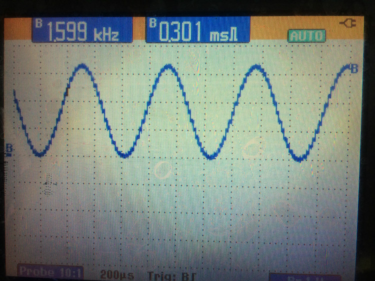
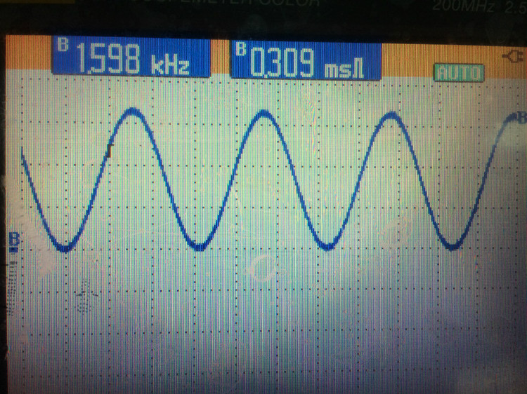
#define _1600Hz (u16)(72000000/sizeof(Sine12bit)*2/1600) //1600Hz
3100 , 3143
, 3185, 3227, 3267, 3307, 3347, 3385, 3423, 3460, 3496, 3531, 3565, 3594, 3631,
3642, 3690, 3737, 3785, 3831, 3877, 3923, 3968, 3013, 3057, 3100, 3143, 3185,
3227, 3267, 3307, 3347, 3385, 3423,
3460, 3496, 3531, 3565, 3598, 3631, 3662, 3692, 3722,
3750, 3778, 3804, 3829, 3854, 3877, 3899, 3920, 3940, 3958, 3976,
3992, 4007, 4021, 4034, 4046, 4056, 40 65, 4073, 4080, 4086
, 4090, 4093, 4095, 4095, 4095, 4093, 4090, 4086, 4080, 4073
, 4065, 4056, 4046, 4034, 4021, 4007, 3992, 3976, 3958,
3940, 3920, 3899, 3877, 3854, 3829, 3804, 3778, 3750, 3722, 3692, 3662
, 3631, 3598, 3565, 3531, 3496, 3460, 34 23, 3385, 3347, 3307
, 3267, 3227, 3185, 3143, 3100, 3057, 3013, 2968, 2923,
2877, 2831, 2785, 2737, 2690, 2642, 2594, 2545, 2496,
2447, 2398, 2348, 2298, 2248, 2198, 2148, 2098, 2047, 1997, 1947, 1897,
1847, 1797, 1747, 1697, 1648, 1599, 1550, 15 01, 1453
, 1405, 1358, 1310, 1264, 1218, 1172, 1127, 1082, 1038,
995, 952, 910, 868, 828, 788, 748, 710, 672, 635,
599, 564, 530, 497, 464, 433, 403, 373, 345, 317,
291, 266, 241, 218, 196, 175, 155, 137, 119, 103,
88, 74, 61, 49, 39, 30, 22, 15, 9, 5,
2, 0, 0, 0, 2, 5, 9, 15, 22, 30,
39, 49, 61, 74, 88, 103, 119, 137, 155, 175,
196, 218, 241, 266, 291, 317, 345, 373, 1797,
1847, 1897, 1947, 1997 }; // const u16 Sine12bit[32] = { // sine 12bit, 16bit, 2047, 2048, 2049, 2050, 2060, 2072, 2080, 2092,
2127, 2172, 2218, 2264,
1310, 1358, 1405, 1453, 1501, 1550, 1599, 1648, 1697, 1747
, 1797, 1847, 1897, 1947, 1997 };
// const u16 Sine12bit[32] = { // sine 12bit, 16bit, 2047, 2080
, 2092, 2080, 2092 2447, 2831, 3185, 3498, 3750, 3939, 4056, 4095, 4056,
// 3939, 3750, 3495, 3185, 2831, 2447, 2047, 1647, 1263, 909,
// 599, 34 4, 155, 38, 0, 38, 155, 344, 599, 909, 1263, 1647};
/****************************************************************
Function: SineWave_TIM_Config
Description: Timer configuration
Input: none
return: none
**************************************************************/
static void SineWave_TIM_Config(void)
{
TIM_TimeBaseInitTypeDef TIM_TimeBaseStructure;
RCC_APB1PeriphClockCmd(RCC_APB1Periph_TIM2|RCC_APB1Periph_TIM6, ENABLE);//Initialize the clocks of timer 2 and
6TIM_TimeBaseStructInit(&TIM_TimeBaseStructure);
TIM_TimeBaseStructure.TIM_Period = _800Hz; //Set the frequency of sine wave
1TIM_TimeBaseStructure.TIM_Prescaler = 0x0; //No pre-
scalingTIM_TimeBaseStructure.TIM_ClockDivision = 0x0; //No clock
divisionTIM_TimeBaseStructure.TIM_CounterMode = TIM_CounterMode_Up;//Increase
countTIM_TimeBaseInit(TIM2, &TIM_TimeBaseStructure);
TIM_TimeBaseStructure.TIM_Period = _1600Hz; //Set sine wave 2 frequency
TIM_TimeBaseInit(TIM6, &TIM_TimeBaseStructure);
TIM_SelectOutputTrigger(TIM2, TIM_TRGOSource_Update); //Update TIM2 output trigger
TIM_SelectOutputTrigger(TIM6, TIM_TRGOSource_Update); //Update TIM6 output trigger
}
/****************************************************************
Function: SineWave_DAC_Config
Description: DAC configuration
Input: none
return: none
*************************************************************/
static void SineWave_DAC_Config(void)
{
DAC_InitTypeDef DAC_InitStructure;
RCC_APB1PeriphClockCmd(RCC_APB1Periph_DAC, ENABLE);//Initialize DAC clock
DAC_StructInit(&DAC_InitStructure);
DAC_InitStructure.DAC_Trigger = DAC_Trigger_T2_TRGO;//Specify trigger timer TIM2 for DAC1
DAC_InitStructure.DAC_WaveGeneration = DAC_WaveGeneration_None;//No waveform generation
DAC_InitStructure.DAC_OutputBuffer = DAC_OutputBuffer_Disable; //Not enable DAC output buffer
DAC_Init(DAC_Channel_1, &DAC_InitStructure); //Initialize DAC channel1
DAC_InitStructure.DAC_Trigger = DAC_Trigger_T6_TRGO; //Specify trigger timer TIM6 for DAC2
DAC_Init(DAC_Channel_2, &DAC_InitStructure); //Initialize DAC channel2
DAC_Cmd(DAC_Channel_1, ENABLE); //Enable DAC channel1
DAC_Cmd(DAC_Channel_2, ENABLE); //Enable DAC channel2
DAC_DMACmd(DAC_Channel_1, ENABLE); //Enable DMA for DAC Channel1
DAC_DMACmd(DAC_Channel_2, ENABLE); //Enable DMA for DAC Channel2
}

#define DAC_DHR12R1 0x40007408 //Base address of peripheral DAC channel 1
#define DAC_DHR12R2 0x40007414 //Base address of peripheral DAC channel 2
/****************************************************************
Function: SineWave_DMA_Config
Description: DMA configuration
Input: none
return: none
**********************************************************/
static void SineWave_DMA_Config(void)
{
DMA_InitTypeDef DMA_InitStructure;
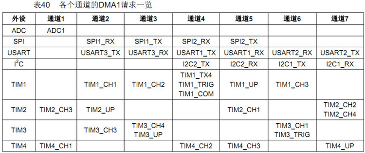
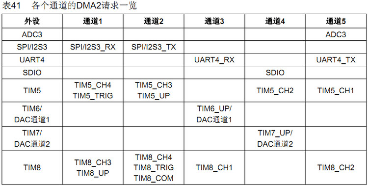
RCC_AHBPeriphClockCmd(RCC_AHBPeriph_DMA2, ENABLE);//Initialize DMA2 clock
DMA_DeInit(DMA2_Channel3); //Configure DMA to default values
DMA_InitStructure.DMA_PeripheralBaseAddr = DAC_DHR12R1;//Specify the target address of DMA2 channel 3 as DAC1_DHR12R1
DMA_InitStructure.DMA_MemoryBaseAddr = (uint32_t)&Sine12bit;//Specify the source address of DMA as array Sine12bit
DMA_InitStructure.DMA_DIR = DMA_DIR_PeripheralDST; //Peripheral as the destination of data transferDMA_InitStructure.DMA_BufferSize
= sizeof(Sine12bit)/2; //DMA buffer sizeDMA_InitStructure.DMA_PeripheralInc
= DMA_PeripheralInc_Disable; //Peripheral machine address register unchangedDMA_InitStructure.DMA_MemoryInc
= DMA_MemoryInc_Enable; //Memory address register incrementDMA_InitStructure.DMA_PeripheralDataSize
= DMA_PeripheralDataSize_HalfWord; //Peripheral data width is half
wordDMA_InitStructure.DMA_MemoryDataSize = DMA_MemoryDataSize_HalfWord; //Memory data width is half
wordDMA_InitStructure.DMA_Mode = DMA_Mode_Circular; //Work in circular cache mode. When the number of data transfers is 0, the initial configuration value is automatically restored
DMA_InitStructure.DMA_Priority = DMA_Priority_VeryHigh; //Very high priority
DMA_InitStructure.DMA_M2M = DMA_M2M_Disable; //The channel is not set to memory-to-memory mode, which is opposite to the circular mode
DMA_Init(DMA2_Channel3, &DMA_InitStructure); //Initialize DMA
DMA_DeInit(DMA2_Channel4);
DMA_InitStructure.DMA_PeripheralBaseAddr = DAC_DHR12R2; //Specify the target address of DMA2 channel 3 as DAC2_DHR12R2
DMA_InitStructure.DMA_Priority = DMA_Priority_VeryHigh;
DMA_Init(DMA2_Channel4, &DMA_InitStructure);
DMA_Cmd(DMA2_Channel3, ENABLE); //Enable DMA channel3
DMA_Cmd(DMA2_Channel4, ENABLE); //Enable DMA channel4
}


DAC_DHR12R1: 12-bit right-aligned data holding register for DAC channel 1 (offset: 0x08)
DAC_DHR12R2: 12-bit right-aligned data holding register for DAC channel 2 (offset: 0x14)
/****************************************************************
Function: SineWave_Init();
Description: Sine wave initialization
Input: none
return: none
*************************************************************/
void SineWave_Init(void)
{
SineWave_GPIO_Config(); //Configure pins
SineWave_TIM_Config(); //Configure timer
SineWave_DAC_Config(); //Configure DAC
SineWave_DMA_Config(); //Configure DMA
TIM_Cmd(TIM2, ENABLE); //Turn on TIM2
TIM_Cmd(TIM6, ENABLE); //Turn on TIM6
}
/****************************************************** ************
Function: main
Description: mainInput
: none
return: none
************************* ************************************/
int main(void)
{
BSP_Init();
SineWave_Init() ;
PRINTF("\nmain() is running!\r\n");
while(1)
{
LED1_Toggle();
Delay_ms(1000);
}
}


Previous article:STM32 ADC conversion
Next article:STM32 external interrupt analysis
- Popular Resources
- Popular amplifiers
- Learn ARM development(16)
- Learn ARM development(17)
- Learn ARM development(18)
- Embedded system debugging simulation tool
- A small question that has been bothering me recently has finally been solved~~
- Learn ARM development (1)
- Learn ARM development (2)
- Learn ARM development (4)
- Learn ARM development (6)
 Professor at Beihang University, dedicated to promoting microcontrollers and embedded systems for over 20 years.
- LED chemical incompatibility test to see which chemicals LEDs can be used with
- Application of ARM9 hardware coprocessor on WinCE embedded motherboard
- What are the key points for selecting rotor flowmeter?
- LM317 high power charger circuit
- A brief analysis of Embest's application and development of embedded medical devices
- Single-phase RC protection circuit
- stm32 PVD programmable voltage monitor
- Introduction and measurement of edge trigger and level trigger of 51 single chip microcomputer
- Improved design of Linux system software shell protection technology
- What to do if the ABB robot protection device stops
- The US asked TSMC to restrict the export of high-end chips, and the Ministry of Commerce responded
- The US asked TSMC to restrict the export of high-end chips, and the Ministry of Commerce responded
- ASML predicts that its revenue in 2030 will exceed 457 billion yuan! Gross profit margin 56-60%
- Detailed explanation of intelligent car body perception system
- How to solve the problem that the servo drive is not enabled
- Why does the servo drive not power on?
- What point should I connect to when the servo is turned on?
- How to turn on the internal enable of Panasonic servo drive?
- What is the rigidity setting of Panasonic servo drive?
- How to change the inertia ratio of Panasonic servo drive
- 【STM32WB55 Review】_05_UART register configuration experiment
- Choosing the right bypass capacitor for high-speed circuit design
- Summary: littleshrimp plays with domestic FPGA (Gaoyun)
- EEWORLD University Hall--In-depth and Easy-to-understand FPGA Video Tutorial 2020 Edition (Privileged Students)
- Lesson 2: Basic knowledge of 5G standards
- Xunwei i.MX6ULL Terminator Process Basics - Process Creation
- Realization of Chinese Characters and Graphics Overlay Based on DSP
- TinyGo releases version 0.11.0
- PID learning materials, motor speed control and proteus simulation
- Today at 10:00 AM TI Live: Industry's Most Accurate 3D Hall Effect Position Sensor

 MAX40010TAUT+T


 京公网安备 11010802033920号