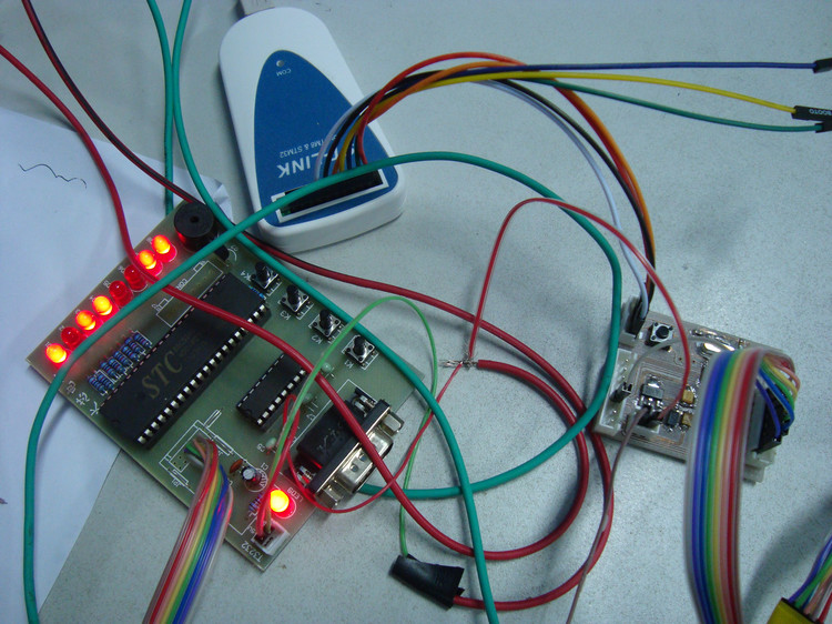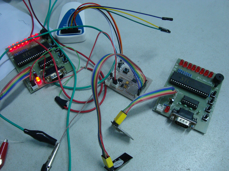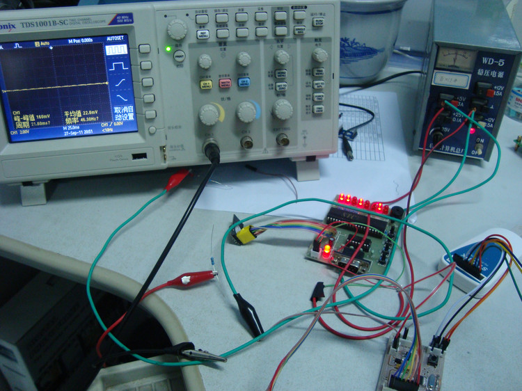


Source program:
/************ STM8S103F learning************************/
/*Chip model: STM8S103F3PB6 */
/*Function description: nrf24l01 wireless module application */ /
*Author: ClimberWin */
/*Written time: 2011.9.25 */
/*Internal crystal oscillator */
/**************************************************/
//Modified time 2011.9.27
//The program was successfully transplanted from C51 to STM8
#include
#define uint unsigned int
#define uchar unsigned char
//********************************************IO port definition***************************************
//****************************************NRF24L01 port definition********************************
/////////////Pin definition//////////////
#define CE PD_ODR_ODR3
#define CSN PD_ODR_ODR2
#define SCK PC_ODR_ODR7
#define MOSI PC_ODR_ODR6
#define MISO PC_IDR_IDR5 //输入
#define IRQ PD_IDR_IDR4 //输入
/******************NRF24L01 partial program**********************/
#define TX_ADR_WIDTH 5 // 5 uints TX address width
#define RX_ADR_WIDTH 5 // 5 uints RX address width
#define TX_PLOAD_WIDTH 20 // 20 uints TX payload
#define RX_PLOAD_WIDTH 20 // 20 uints TX payload
uchar TX_ADDRESS[TX_ADR_WIDTH]= {0x12,0x34,0x56,0x78,0x9 0} ; //Local address
uchar RX_ADDRESS[RX_ADR_WIDTH]= {0x12,0x34,0x56,0x78,0x90}; //Receive address
//****************************************NRF24L01 register instruction** ************************************************** ***
#define READ_REG 0x00 // Read register instruction
#define WRITE_REG 0x20 // Write register instruction
#define RD_RX_PLOAD 0x61 // Read receive data instruction
#define WR_TX_PLOAD 0xA0 // Write data to be sent instruction
#define FLUSH_TX 0xE1 // Flush Send FIFO instruction
#define FLUSH_RX 0xE2 // Flush receive FIFO instruction
#define REUSE_TX_PL 0xE3 // Define repeat load data instruction
#define NOP 0xFF // Reserved
//******************** ********************SPI(nRF24L01)Register Address**************************** ****************************
#define CONFIG 0x00 // Configure the receiving and sending status, CRC check mode and receiving and sending status response mode
#define EN_AA 0x01 // Automatic answer function setting
#define EN_RXADDR 0x02 // Available channel setting
#define SETUP_AW 0x03 // Send and receive address width setting
#define SETUP_RETR 0x04 // Automatic reset Transmit function settings
#define RF_CH 0x05 // Operating frequency settings
#define RF_SETUP 0x06 // Transmit rate, power consumption function settings
#define STATUS 0x07 // Status register
#define OBSERVE_TX 0x08 // Transmit monitoring function
#define CD 0x09 // Address detection
#define RX_ADDR_P0 0x0A // Channel 0 receive data address
#define RX_ADDR_P1 0x0B // Channel 1 receive data address
#define RX_ADDR_P2 0x0C // Channel 2 receive data address
#define RX_ADDR_P3 0x0D // Channel 3 receive data address
#define RX_ADDR_P4 0x0E // Channel 4 receive data address
#define RX_ADDR_P5 0x0F // Channel 5 receive data address
#define TX_ADDR 0x10 // Transmit address register
#define RX_PW_P0 0x11 // Receive data length for receiving channel 0
#define RX_PW_P1 0x12 // Receive data length for receiving channel 0
#define RX_PW_P2 0x13 // Receive data length for receiving channel 0
#define RX_PW_P3 0x14 // Receive data length for receiving channel 0
#define RX_PW_P4 0x15 / / Receive data length for receiving channel 0
#define RX_PW_P5 0x16 // Receive data length for receiving channel 0
#define FIFO_STATUS 0x17 // FIFO stack push and pull status register settings
void init_NRF24L01(void);
volatile SPI_RW(volatile byte);
volatile SPI_Read(volatile reg);
void SetRX_Mode(void);
fly SPI_RW_Reg(fly reg, fly value);
fly SPI_Read_Buf(fly reg, fly *pBuf, fly num);
fly SPI_Write_Buf(fly reg, fly *pBuf, fly num);
unsigned char nRF24L01_RxPacket(unsigned char* rx_buf);
void nRF24L01_TxPacket(unsigned char * tx_buf);
void IO_config(void);
void delayms(unsigned int count);
flying sta;
#define RX_DR (sta & 0x40)
#define TX_DS (sta & 0x20)
#define MAX_RT (sta & 0x10)
void delayms(unsigned int count)
{
unsigned int i,j;
for(i=0;i
}
//NRF24L01 initialization
void init_NRF24L01(void)
{
delayms(1);
CE=0; // chip enable
CSN=1; // Spi disable
SCK=0; // Spi clock line init high
SPI_Write_Buf(WRITE_REG + TX_ADDR, TX_ADDRESS, TX_ADR_WIDTH); // Write local address
SPI_Write_Buf(WRITE_REG + RX_ADDR_P0, RX_ADDRESS, RX_ADR_WIDTH); // Write receiving address
SPI_RW_Reg(WRITE_REG + EN_AA, 0x01); // Channel 0 automatic ACK response allowed
SPI_RW_Reg(WRITE_REG + EN_RXADDR, 0x01); // Only channel 0 is allowed to receive address. If multiple channels are needed, please refer to Page21
SPI_RW_Reg(WRITE_REG + RF_CH, 0); // Set the channel to work at 2.4GHZ, and the transmission and reception must be consistent
SPI_RW_Reg(WRITE_REG + RX_PW_P0, RX_PLOAD_WIDTH); //Set the length of the received data, this time it is set to 32 bytes
SPI_RW_Reg(WRITE_REG + RF_SETUP, 0x07); //Set the transmission rate to 1MHZ and the transmission power to the maximum value 0dB
}
//Function: uint SPI_RW(uint uchar)
//Function: SPI write timing of NRF24L01
uchar SPI_RW(uchar byte)
{
uchar i;
for(i=0;i<8;i++) // output 8-bit
{
if((byte & 0x80)==0)
{MOSI=0;}
else
{MOSI=1;}
byte = (byte << 1); // shift next bit into MSB..
SCK = 1; // Set SCK high..
if(MISO == 0)
{byte |= 0;} // capture current MISO bit
else
{byte |= 1;}
SCK = 0; // ..then set SCK low again
}
return(byte); // return read uchar
}
/*uchar SPI_RW(uchar byte)
{
uchar i;
for(i=0;i<8;i++) // output 8-bit
{
MOSI = (byte & 0x80); // output 'uchar', MSB to MOSI
byte = (byte << 1); // shift next bit into MSB..
SCK = 1; // Set SCK high..
byte |= MISO; // capture current MISO bit
SCK = 0; // ..then set SCK low again
}
return(byte); // return read uchar
}*/
//Function: uchar SPI_Read(uchar reg)
//Function: SPI timing of NRF24L01
uchar SPI_Read(uchar reg)
{
uchar reg_val;
CSN = 0; // CSN low, initialize SPI communication...
SPI_RW(reg); // Select register to read from..
reg_val = SPI_RW(0); // ..then read registervalue
CSN = 1; // CSN high, terminate SPI communication
return(reg_val); // return register value
}
//Function: NRF24L01 read and write register function
uchar SPI_RW_Reg(uchar reg, uchar value)
{
uint status;
CSN = 0; // CSN low, init SPI transaction
status = SPI_RW(reg); // select register
SPI_RW(value); // ..and write value to it..
CSN = 1; // CSN high again
return(status); // return nRF24L01 status uchar
}
//Function: uint SPI_Read_Buf(uchar reg, uchar *pBuf, uchar uchars)
//Function: used to read data, reg: register address, pBuf: address of data to be read, uchars: number of data to be read
uchar SPI_Read_Buf(uchar reg, uchar *pBuf, uchar num)
{
uchar status,i;
CSN = 0; // Set CSN low, init SPI tranaction
status = SPI_RW(reg); // Select register to write to and read status uchar
for(i=0;i
CSN = 1;
return(status); // return nRF24L01 status uchar
}
//Function: uint SPI_Write_Buf(uchar reg, uchar *pBuf, uchar uchars)
//Function: used to write data: register address, pBuf: address of data to be written, uchars: number of data to be written
uchar SPI_Write_Buf(uchar reg, uchar *pBuf, uchar num)
{
uchar status,i;
CSN = 0; //SPI enable
status = SPI_RW(reg);
for(i=0; i
CSN = 1; //Close SPI
return(status); //
}
//Function: void SetRX_Mode(void)
//Function: Data receiving configuration
void SetRX_Mode(void)
{
CE=0;
SPI_RW_Reg(WRITE_REG + CONFIG, 0x0f); // IRQ reception and transmission completion interrupt response, 16-bit CRC, main reception
CE = 1;
delayms(1);
}
/******************************************************************************************************/
//Function: unsigned char nRF24L01_RxPacket(unsigned char* rx_buf)
//Function: After reading data, put it in the rx_buf receiving buffer
unsigned char nRF24L01_RxPacket(unsigned char* rx_buf)
{
unsigned char revale=0;
sta=SPI_Read(STATUS); // Read the status register to determine the data reception status
if(RX_DR) // Determine whether data is received
{
CE = 0; //SPI enables
SPI_Read_Buf(RD_RX_PLOAD,rx_buf,TX_PLOAD_WIDTH);// read receive payload from RX_FIFO buffer
revale =1; //Read data completion flag
}
SPI_RW_Reg(WRITE_REG+STATUS,sta); //After receiving the data, RX_DR,TX_DS,MAX_PT are all set high to 1, and the interrupt flag is cleared by writing 1
return revale;
}
//Function: void nRF24L01_TxPacket(unsigned char * tx_buf)
//Function: Send data in tx_buf
void nRF24L01_TxPacket(unsigned char * tx_buf)
{
CE=0; //StandBy I mode
SPI_Write_Buf(WRITE_REG + RX_ADDR_P0, TX_ADDRESS, TX_ADR_WIDTH); //Load receiving end address
SPI_Write_Buf(WR_TX_PLOAD, tx_buf, TX_PLOAD_WIDTH); //Load data
SPI_RW_Reg(WRITE_REG + CONFIG, 0x0e); //IRQ transceiver completion interrupt response, 16-bit CRC, master send
CE=1; //Set CE high to stimulate data transmission
delayms(1);
}
//***********Port configuration******************/
void IO_config(void)
{
PC_DDR_DDR5=0;
PC_DDR_DDR6=1;
PC_DDR_DDR7=1;
PD_DDR_DDR2=1;
PD_DDR_DDR3=1;
PD_DDR_DDR4=0;
PC_CR1_C15=1;//Input pull-up
PC_CR1_C16=1;
PC_CR1_C17=1;
PD_CR1_C12=1;
PD_CR1_C13=1;
PD_CR1_C14=0;//Input pull-up
PC_CR2 = 0x00;
PD_CR2 = 0x00;
}
/***********************************/
/*****************主程序********************/
void main(void)
{
unsigned char TxBuf[20]={0}; //
unsigned char RxBuf[20]={0};
unsigned char led_num;
// unsigned char rx_temp;
delayms(100);
IO_config();
init_NRF24L01() ;
TxBuf[1] =0x55 ;
nRF24L01_TxPacket(TxBuf); // Transmit Tx buffer data
delayms(1000);
led_num=0x00;
while(1)
{
TxBuf[1] =led_num ;
nRF24L01_TxPacket(TxBuf); // Transmit Tx buffer data
led_num++;
delayms(500);
//***************************************************************************************************
SetRX_Mode(); // Start sending each time and then jump directly to receiving without pressing a button, and keep looping.
nRF24L01_RxPacket(RxBuf);
if(RX_DR==0)
{
// rx_temp=0x55;
delayms(10);
}
else
{
delayms(10);
}
}
}
Previous article:STM8S103F2 NOKIA5110+AD acquisition
Next article:STM8S103F---Nokia5110 LCD display
Recommended ReadingLatest update time:2024-11-16 00:05


- Popular Resources
- Popular amplifiers
-
 STM8 C language programming (1) - basic program and startup code analysis
 -
 Description of the BLDC back-EMF sampling method based on the STM8 official library
 -
 STM32 MCU project example: Smart watch design based on TouchGFX (8) Associating the underlying driver with the UI
 -
 uCOS-III Kernel Implementation and Application Development Practical Guide - Based on STM32 (Wildfire)
 Professor at Beihang University, dedicated to promoting microcontrollers and embedded systems for over 20 years.
- Allegro MicroSystems Introduces Advanced Magnetic and Inductive Position Sensing Solutions at Electronica 2024
- Car key in the left hand, liveness detection radar in the right hand, UWB is imperative for cars!
- After a decade of rapid development, domestic CIS has entered the market
- Aegis Dagger Battery + Thor EM-i Super Hybrid, Geely New Energy has thrown out two "king bombs"
- A brief discussion on functional safety - fault, error, and failure
- In the smart car 2.0 cycle, these core industry chains are facing major opportunities!
- The United States and Japan are developing new batteries. CATL faces challenges? How should China's new energy battery industry respond?
- Murata launches high-precision 6-axis inertial sensor for automobiles
- Ford patents pre-charge alarm to help save costs and respond to emergencies
- New real-time microcontroller system from Texas Instruments enables smarter processing in automotive and industrial applications
- I decided to quit my job and develop my operating system full-time (transferred)
- Design rules for four-layer PCB
- If there is no reference ground at all, do you think it is still possible to control the impedance?
- Why is the stm32 pin reading different from the oscilloscope measurement?
- msp430f5529 uart pwm adc
- Please help me how to install the PIC software EPOCH. The csdn is very vague and I have never seen the operation described in the installation instructions.
- Understanding NB-IoT technology
- 3DH Model
- What kind of products need a dedicated shutdown discharge circuit?
- [First Round] Interview Questions for Embedded Engineers

 STM8 C language programming (1) - basic program and startup code analysis
 Description of the BLDC back-EMF sampling method based on the STM8 official library


 京公网安备 11010802033920号