1. PHASE LOCKED LOOP (PLL)
S3C6410 contains three PLLs (phase-locked loops), APLL, MPLL, and EPLL. By setting them, the input clock is synchronized and output to achieve the purpose of operating the CPU's operating frequency. As shown in Figure 1-1.
The Voltage Controlled Oscillator (VCO) P[5:0] bit is used to set FIN for frequency division. By setting the Main-Divider frequency division number, the output clock frequency generated by the frequency-divided voltage-controlled oscillator, and the low frequency after frequency division enters the phase detector Scaler S[2:0] bit to set the output clock frequency of the PLL, all of which can be selected through
the PLL clock selection and input reference clock.
Figure 1-2 describes the clock generation logic. S3C6410 has three PLL phase-locked loops, and the working clock is also divided into three groups. APLL is used to provide working clocks for ARM chips, MPLL provides working clocks for devices on AXI, AHB, and APB buses, and EPLL provides working clocks for special peripherals, such as video decoders, picture encoders, etc.
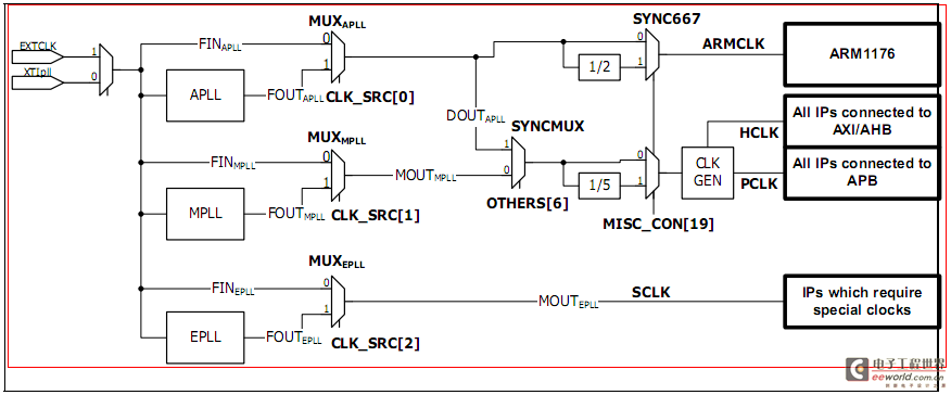
Figure 1-2 Clock Generation Logic Unit
The lower three bits of the CLK_SRC register CLK_SRC[2:0] control three working clocks respectively. When the corresponding bit is set, the corresponding PLL working clock is generated. Otherwise, the corresponding PLL working clock will not be generated.
3. Generation of three working clocks
ARM1176 generates a maximum working frequency of 667Mhz. Users can control the output working clock by setting the value of the internal clock divider without modifying the working frequency of the PLL. The divider can select a division number of 1 to 16. The ARM core can reduce the power consumption of the system by modifying the value of the divider.
S3C6410 contains AXI, AHB and APB buses. Different buses control different peripherals. Turning off the clock frequency on the bus can achieve the purpose of system energy saving. The AXI and AHB buses work at a maximum frequency of 133MHz, and the APB bus works at a maximum frequency of 66MHz. Since the working frequencies of the APB and AXI, AHB buses are inconsistent, special logic units are used when data is transmitted synchronously on these two buses, as shown in Figure 1-3.
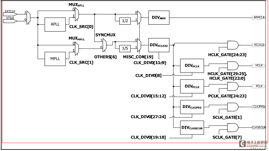
Figure 1-3 System bus operating frequency setting
The HCLKX2 clock is generated by the two DDR controllers DDR0 and DDR1, and can send and receive data at a maximum frequency of 266MHz. Each HCLKX2 clock can be turned off according to user needs to reduce system loss. The clock on the AHB bus is divided and output by the DIV (HCLK) divider. Similarly, the peripherals on the AHB bus can also be turned off to save power consumption. The HCLK_GATE register is used to turn off peripherals working on the HCLKX2 and HCLK clocks.
Slow devices are connected to the APB bus. The APB clock works at a maximum of 66MHz, and the frequency division is set by the DIV (PCLk) divider. The corresponding peripherals on the APB bus are turned off by setting the PCLK_GATE register. According to the S3C6410 hardware manual, the frequencies on the AHB bus and APB bus must be even numbers. For example, if the control bit CLK_DIV[8] corresponding to DIV(HCLK) is set to 1, the corresponding bit CLK_DIV0[15:12] of DIV(PCLK) must be set to an odd number such as 1, 3, 5, ... Otherwise, the peripherals on the APB bus cannot perform data transmission correctly. The
JPEG and security-related subsystems on the AHB bus cannot operate at 133MHz. The AHB bus provides a low-frequency working clock for such low-frequency subsystems, and sets its operating frequency by setting the DIV(CLKJPEG) and DIV(CLKSECUR) division bits. Therefore, there are similar restrictions on the APB bus. The CLK_DIV0[27:24] division bits and CLK_DIV0[19:18] division bits corresponding to DIV(CLKJPEG) and DIV(CLKSECUR) must be odd numbers, and the sum of the two is an even number. As shown in Table 1-1, the official recommended setting parameters are given.
Table 1-1 Official recommended parameters

4. Generation of MFC module clock
The MFC module requires a special clock, as shown in Figure 1-5.

Figure 1-5 MFC clock generation logic
The MFC clock source can be selected from HCLKX2 and MOUT (EPLL). The working clock of the MFC uses HCLKX2 to divide the frequency. The default HCLKX2 clock frequency is 266MHz. Therefore, CLK_DIV0[31:28] must be set to b0001 to generate a 133MHz clock for the MFC to work. When the MFC module does not need to work in high-performance mode, there are two ways to reduce the operating frequency of the MFC module to reduce the power consumption of the MFC module. The first way is to set CLK_SRC[4] to use the output clock of EPLL. The other way is to set the division number of CLK_DIV0[31:28] and set the CLK_SRC[4] bit at the same time, so that the low-frequency working clock can be provided to the MFC module. The EPLL output clock is independent of HCLKX2 and HCLK.
5. Generation of UART, SPI, and MMC working clocks
As shown in Figure 1-6, the working clock logic of the above three peripherals is shown.
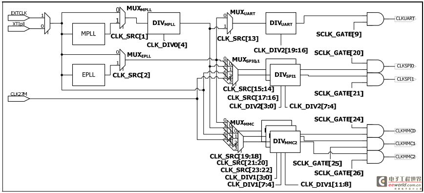
Figure 1-6 UART, SPI, and MMC working clock logic module
The division number of the UART working frequency is set by setting the CLK_DIV2[19:16] bit, and the UART clock source is turned on and off by SCLK_GATE[9].
There is an additional clock source CLK27M in this module, which can provide more optional working clocks.
6. Clock on/off control
HCLK_GATE, PCLK_GATE, and SCLK_GATE are used to control the generation of three clock sources. If the corresponding bit is set, the corresponding clock will be generated.
HCLK_GATE controls the generation of peripheral working clocks on the HCLK bus, and PCLK_GATE controls the generation of peripheral working clocks on the PCLK bus. Peripherals on the PCLK bus require specific clocks, which are set by SCLK_GATE.
7. Synchronous 667MHz operation mode
According to the S3C6410 hardware manual, the clock ratio of ARMCLK and HCLK must be an integer to synchronize the clocks of the ARM core and the AXI bus interface. S3C6410 does not limit the CPU to work at 533MHz, ARMCLK = 533MHz, HCLKX2 = 266MHz, HCLK = 133MH, but when working above 533MHz, such as 667Mhz, it can only support a clock ratio of 1:2.5:5 (ARMCLK = 667MHz, HCLKX2 = 266MHz, HCLK = 133MH)
8. Clock division

Figure 1-7 Clock division module
As shown in Figure 1-7, the clock divider module generates three clocks, ARMCLK, HCLKX2, and HCLK. The clock divider consists of two parts, the pre-divider group and the post-divider group. The pre-divider includes a 1/2 pre-divider and a 1/5 pre-divider. These two dividers are fixed and cannot be configured by software, while the post-divider can be configured by configuring the CLK_DIV0 register. When the SYNC667MHz bit of MISC_CON is set, the two pre-dividers work at the same time to generate the APLL's divided clock after the pre-divider. If the FOUT output frequency of the APLL is 1.33GHz, the output of the pre-divider ARMCLK is 667Mhz, and the output of the pre-divider HCLK is 266MHz. The divided clock can be configured through the CLK_DIV0 register.
We intend to set the ARM core clock to the officially recommended stable 533MHz, and let APLL output the operating frequency for AHB and APB. Let MPLL provide the operating frequency for UART and other peripherals, and EPLL does not work. At the same time, set HCLKX2 to 266MHz, HCLK to 133MHz, PCLK to 66.5MHz, and the UART operating clock is 66.5MHz.
1. Select the clock source of HCLKX2, HCLK, and PCLK. As shown in Figure 1-2, the clock source can be selected from DOUT_APLL or MOUT_MPLL through OTHER[6]. We choose DOUT_APLL.
2. Set the frequency conversion lock time. After the system clock is modified, a LOCK time period must pass.
3. Set the frequency division of ARMCLK, HCLKX2, HCLK, PCLK
The relationship between various frequencies is shown in Figure 1-3:
The output frequency generated by APLL or MPLL is selected by OTHER[6] and then selected by MISC_CON[19] to be divided by 1/5. The generated output frequency enters DIV_HCLKx2. The output frequencies of HCLKX2, HCLK, PCLK, CLKJPEG, and CLKSECUR are set according to the different bits of CLK_DIV0. The value setting is described in the description of the CLK_DIV0 register.
l We select DOUT_APLL for MPLL, and MISC_ON[19] does not divide the frequency. The clock (533MHz) generated by DOUT_APLL directly enters the DIV_HCLKX2 divider.
l According to the hardware manual, the frequency of HCLKX2 is fixed at 266MHz, so HCLKX2_RATIO is set to 0b1
l There is memory connected to HCLK, and the maximum operating frequency of Mobile DDR memory is 133MHz, so the maximum main frequency of HCLK is set to 1/2 of HCLKX2, that is: HCLK_RATIO = 0b1
l Set the operating frequency on PCLK to 66.5MHz, that is: PCLK_RATIO = 0b11
l Set the operating frequency of ARM core to 553MHz, that is: ARM_RATIO = 0b0
l Set DOUT_MPLL to 266MHz to provide a clock source for the subsequent UART, that is: MPLL_RATIO = 0b0
l Keep other clock frequencies at the default values
4. Set UART working clock
As shown in Figure 1-6, CLK_SRC[1] is set to select whether to multiply the working clock of DOUT_MPLL, CLK_DIV0[4] is set to divide the clock, CLK_SRC[13] is used to select the working clock source of UART, and CLK_DIV2[19:16] is set to divide the working clock of UART. As shown in the previous figure, DOUT_MPLL = 266MHz, and UART selects it as its working clock source. Then, dividing it by 1/4 can get 66.5MHz.
As shown in the following table: Set register CLK_DIV2[19:16] = 0b11, and set CLK_SRC[13] = 0b1.
5. Enable APLL and EPLL phase-locked loops
Set the M, D, and S frequency divisions of APLL and EPLL according to the instructions in the hardware manual.
APLL generates FOUT_APLL of 533MHz and
EPLL generates MOUT_EPLL of 266MHz
6. Set the corresponding clock source register to provide clock frequency for various peripherals
Keywords:S3C6410
Reference address:S3C6410 clock initialization
S3C6410 contains three PLLs (phase-locked loops), APLL, MPLL, and EPLL. By setting them, the input clock is synchronized and output to achieve the purpose of operating the CPU's operating frequency. As shown in Figure 1-1.
The Voltage Controlled Oscillator (VCO) P[5:0] bit is used to set FIN for frequency division. By setting the Main-Divider frequency division number, the output clock frequency generated by the frequency-divided voltage-controlled oscillator, and the low frequency after frequency division enters the phase detector Scaler S[2:0] bit to set the output clock frequency of the PLL, all of which can be selected through
the PLL clock selection and input reference clock.
Figure 1-2 describes the clock generation logic. S3C6410 has three PLL phase-locked loops, and the working clock is also divided into three groups. APLL is used to provide working clocks for ARM chips, MPLL provides working clocks for devices on AXI, AHB, and APB buses, and EPLL provides working clocks for special peripherals, such as video decoders, picture encoders, etc.

Figure 1-2 Clock Generation Logic Unit
The lower three bits of the CLK_SRC register CLK_SRC[2:0] control three working clocks respectively. When the corresponding bit is set, the corresponding PLL working clock is generated. Otherwise, the corresponding PLL working clock will not be generated.
3. Generation of three working clocks
ARM1176 generates a maximum working frequency of 667Mhz. Users can control the output working clock by setting the value of the internal clock divider without modifying the working frequency of the PLL. The divider can select a division number of 1 to 16. The ARM core can reduce the power consumption of the system by modifying the value of the divider.
S3C6410 contains AXI, AHB and APB buses. Different buses control different peripherals. Turning off the clock frequency on the bus can achieve the purpose of system energy saving. The AXI and AHB buses work at a maximum frequency of 133MHz, and the APB bus works at a maximum frequency of 66MHz. Since the working frequencies of the APB and AXI, AHB buses are inconsistent, special logic units are used when data is transmitted synchronously on these two buses, as shown in Figure 1-3.

Figure 1-3 System bus operating frequency setting
The HCLKX2 clock is generated by the two DDR controllers DDR0 and DDR1, and can send and receive data at a maximum frequency of 266MHz. Each HCLKX2 clock can be turned off according to user needs to reduce system loss. The clock on the AHB bus is divided and output by the DIV (HCLK) divider. Similarly, the peripherals on the AHB bus can also be turned off to save power consumption. The HCLK_GATE register is used to turn off peripherals working on the HCLKX2 and HCLK clocks.
Slow devices are connected to the APB bus. The APB clock works at a maximum of 66MHz, and the frequency division is set by the DIV (PCLk) divider. The corresponding peripherals on the APB bus are turned off by setting the PCLK_GATE register. According to the S3C6410 hardware manual, the frequencies on the AHB bus and APB bus must be even numbers. For example, if the control bit CLK_DIV[8] corresponding to DIV(HCLK) is set to 1, the corresponding bit CLK_DIV0[15:12] of DIV(PCLK) must be set to an odd number such as 1, 3, 5, ... Otherwise, the peripherals on the APB bus cannot perform data transmission correctly. The
JPEG and security-related subsystems on the AHB bus cannot operate at 133MHz. The AHB bus provides a low-frequency working clock for such low-frequency subsystems, and sets its operating frequency by setting the DIV(CLKJPEG) and DIV(CLKSECUR) division bits. Therefore, there are similar restrictions on the APB bus. The CLK_DIV0[27:24] division bits and CLK_DIV0[19:18] division bits corresponding to DIV(CLKJPEG) and DIV(CLKSECUR) must be odd numbers, and the sum of the two is an even number. As shown in Table 1-1, the official recommended setting parameters are given.
Table 1-1 Official recommended parameters

4. Generation of MFC module clock
The MFC module requires a special clock, as shown in Figure 1-5.

Figure 1-5 MFC clock generation logic
The MFC clock source can be selected from HCLKX2 and MOUT (EPLL). The working clock of the MFC uses HCLKX2 to divide the frequency. The default HCLKX2 clock frequency is 266MHz. Therefore, CLK_DIV0[31:28] must be set to b0001 to generate a 133MHz clock for the MFC to work. When the MFC module does not need to work in high-performance mode, there are two ways to reduce the operating frequency of the MFC module to reduce the power consumption of the MFC module. The first way is to set CLK_SRC[4] to use the output clock of EPLL. The other way is to set the division number of CLK_DIV0[31:28] and set the CLK_SRC[4] bit at the same time, so that the low-frequency working clock can be provided to the MFC module. The EPLL output clock is independent of HCLKX2 and HCLK.
5. Generation of UART, SPI, and MMC working clocks
As shown in Figure 1-6, the working clock logic of the above three peripherals is shown.

Figure 1-6 UART, SPI, and MMC working clock logic module
The division number of the UART working frequency is set by setting the CLK_DIV2[19:16] bit, and the UART clock source is turned on and off by SCLK_GATE[9].
There is an additional clock source CLK27M in this module, which can provide more optional working clocks.
6. Clock on/off control
HCLK_GATE, PCLK_GATE, and SCLK_GATE are used to control the generation of three clock sources. If the corresponding bit is set, the corresponding clock will be generated.
HCLK_GATE controls the generation of peripheral working clocks on the HCLK bus, and PCLK_GATE controls the generation of peripheral working clocks on the PCLK bus. Peripherals on the PCLK bus require specific clocks, which are set by SCLK_GATE.
7. Synchronous 667MHz operation mode
According to the S3C6410 hardware manual, the clock ratio of ARMCLK and HCLK must be an integer to synchronize the clocks of the ARM core and the AXI bus interface. S3C6410 does not limit the CPU to work at 533MHz, ARMCLK = 533MHz, HCLKX2 = 266MHz, HCLK = 133MH, but when working above 533MHz, such as 667Mhz, it can only support a clock ratio of 1:2.5:5 (ARMCLK = 667MHz, HCLKX2 = 266MHz, HCLK = 133MH)
8. Clock division

Figure 1-7 Clock division module
As shown in Figure 1-7, the clock divider module generates three clocks, ARMCLK, HCLKX2, and HCLK. The clock divider consists of two parts, the pre-divider group and the post-divider group. The pre-divider includes a 1/2 pre-divider and a 1/5 pre-divider. These two dividers are fixed and cannot be configured by software, while the post-divider can be configured by configuring the CLK_DIV0 register. When the SYNC667MHz bit of MISC_CON is set, the two pre-dividers work at the same time to generate the APLL's divided clock after the pre-divider. If the FOUT output frequency of the APLL is 1.33GHz, the output of the pre-divider ARMCLK is 667Mhz, and the output of the pre-divider HCLK is 266MHz. The divided clock can be configured through the CLK_DIV0 register.
We intend to set the ARM core clock to the officially recommended stable 533MHz, and let APLL output the operating frequency for AHB and APB. Let MPLL provide the operating frequency for UART and other peripherals, and EPLL does not work. At the same time, set HCLKX2 to 266MHz, HCLK to 133MHz, PCLK to 66.5MHz, and the UART operating clock is 66.5MHz.
1. Select the clock source of HCLKX2, HCLK, and PCLK. As shown in Figure 1-2, the clock source can be selected from DOUT_APLL or MOUT_MPLL through OTHER[6]. We choose DOUT_APLL.
ldr r0, =CLOCK_BASE ;0x7e00f000
ldr r1, [r0, #OTHERS_OFFSET] ; Select the clock source of MPLL
movr2, #0x40
orr r1, r1, r2
str r1, [r0, #OTHERS_OFFSET]
nop
nop
nop
nop
; Select the synchronous working mode of CPU
ldr r2, =0x80
orr r1, r1, r2
str r1, [r0, #OTHERS_OFFSET]
; Test whether it is working in synchronous mode
check_syncack
ldr r1, [r0, #OTHERS_OFFSET]
ldr r2, =0xf00
and r1, r1, r2
cmpr1, #0xf00
bne check_syncack
2. Set the frequency conversion lock time. After the system clock is modified, a LOCK time period must pass.
; Set the frequency conversion lock time
movr1, #0xff00
orr r1, r1, #0xff
str r1, [r0, #APLL_LOCK_OFFSET]
str r1, [r0, #MPLL_LOCK_OFFSET]
str r1, [r0, #EPLL_LOCK_OFFSET]
movr1, #0xff00
orr r1, r1, #0xff
str r1, [r0, #APLL_LOCK_OFFSET]
str r1, [r0, #MPLL_LOCK_OFFSET]
str r1, [r0, #EPLL_LOCK_OFFSET]
3. Set the frequency division of ARMCLK, HCLKX2, HCLK, PCLK
The relationship between various frequencies is shown in Figure 1-3:
The output frequency generated by APLL or MPLL is selected by OTHER[6] and then selected by MISC_CON[19] to be divided by 1/5. The generated output frequency enters DIV_HCLKx2. The output frequencies of HCLKX2, HCLK, PCLK, CLKJPEG, and CLKSECUR are set according to the different bits of CLK_DIV0. The value setting is described in the description of the CLK_DIV0 register.
l We select DOUT_APLL for MPLL, and MISC_ON[19] does not divide the frequency. The clock (533MHz) generated by DOUT_APLL directly enters the DIV_HCLKX2 divider.
l According to the hardware manual, the frequency of HCLKX2 is fixed at 266MHz, so HCLKX2_RATIO is set to 0b1
l There is memory connected to HCLK, and the maximum operating frequency of Mobile DDR memory is 133MHz, so the maximum main frequency of HCLK is set to 1/2 of HCLKX2, that is: HCLK_RATIO = 0b1
l Set the operating frequency on PCLK to 66.5MHz, that is: PCLK_RATIO = 0b11
l Set the operating frequency of ARM core to 553MHz, that is: ARM_RATIO = 0b0
l Set DOUT_MPLL to 266MHz to provide a clock source for the subsequent UART, that is: MPLL_RATIO = 0b0
l Keep other clock frequencies at the default values
; MPLL_RATIO = 0<<4, ARM_RATIO = 0
; DOUT_MPLL = MOUT_MPLL/(MPLL_RATIO + 1)
; That is, ARMCLK = DOUT_APLL / (ARM_RATIO + 1)
; That is, ARMCLK = 533MHz, DOUT_MPLL = 266MHz
; HCLKX2_RATIO = 1<<9 , HCLK_RATIO = 1<<8, PCLK_RATIO = 3<<12, HCLKX2IN = 533
; That is, HCLKX2 = HCLKX2IN / (HCLKX2_RATIO + 1) = 266
; That is, HCLK = HCLKX2 / (HCLK_RATIO + 1) = 133
; That is, PCLK = HCLKX2 / (PCLK_RATIO + 1) = 66.5
ldr r1, [r0, #CLK_DIV0_OFFSET]
bic r1, r1, #0xff00
bic r1, r1, #0xff
ldr r2, =0x3300
orr r1, r1, r2
str r1, [r0, #CLK_DIV0_OFFSET]
4. Set UART working clock
As shown in Figure 1-6, CLK_SRC[1] is set to select whether to multiply the working clock of DOUT_MPLL, CLK_DIV0[4] is set to divide the clock, CLK_SRC[13] is used to select the working clock source of UART, and CLK_DIV2[19:16] is set to divide the working clock of UART. As shown in the previous figure, DOUT_MPLL = 266MHz, and UART selects it as its working clock source. Then, dividing it by 1/4 can get 66.5MHz.
As shown in the following table: Set register CLK_DIV2[19:16] = 0b11, and set CLK_SRC[13] = 0b1.
; Set the UART serial port division register CLK_DIV2
ldr r1, [r0, #CLK_DIV2_OFFSET]
bic r1, r1, #0x70000
orr r1, r1, #0x30000 ; Set its value to 3, i.e. CLKUART = CLKUARTIN / 4
str r1, [r0, #CLK_DIV2_OFFSET]
ldr r1, [r0, #CLK_DIV2_OFFSET]
bic r1, r1, #0x70000
orr r1, r1, #0x30000 ; Set its value to 3, i.e. CLKUART = CLKUARTIN / 4
str r1, [r0, #CLK_DIV2_OFFSET]
5. Enable APLL and EPLL phase-locked loops
Set the M, D, and S frequency divisions of APLL and EPLL according to the instructions in the hardware manual.
APLL generates FOUT_APLL of 533MHz and
EPLL generates MOUT_EPLL of 266MHz
; Enable APLL phase-locked loop, configure M, D, S frequency division, according to Datasheet FOUT_APLL = 533 then
; APLL_EN = 1<<31, MDIV = 266<<16, PDIV = 3<<8, SDIV = 1
ldr r1, = 0x810a0301
str r1, [r0, #APLL_CON_OFFSET]
; Enable MPLL phase-locked loop, configure M, D, S frequency division
; MPLL_EN = 1<<31, MDIV = 266<<16, PDIV = 3<<8, SDIV = 2
ldr r1, = 0x810a0302
str r1, [r0, #MPLL_CON_OFFSET]
; APLL_EN = 1<<31, MDIV = 266<<16, PDIV = 3<<8, SDIV = 1
ldr r1, = 0x810a0301
str r1, [r0, #APLL_CON_OFFSET]
; Enable MPLL phase-locked loop, configure M, D, S frequency division
; MPLL_EN = 1<<31, MDIV = 266<<16, PDIV = 3<<8, SDIV = 2
ldr r1, = 0x810a0302
str r1, [r0, #MPLL_CON_OFFSET]
6. Set the corresponding clock source register to provide clock frequency for various peripherals
; UART_SEL = 0b1
; MPLL_SEL = 0b1, APLL_SEL = 0b1
ldr r1, [r0, #CLK_SRC_OFFSET]
ldr r2, =0x2005 ; Also set the UART clock source to come from MPLL
orr r1, r1, r2
str r1, [r0, #CLK_SRC_OFFSET]
; MPLL_SEL = 0b1, APLL_SEL = 0b1
ldr r1, [r0, #CLK_SRC_OFFSET]
ldr r2, =0x2005 ; Also set the UART clock source to come from MPLL
orr r1, r1, r2
str r1, [r0, #CLK_SRC_OFFSET]
Previous article:S3C2440 SDRAM memory driver
Next article:ARM9(2440) read and write operations on nand flash
- Popular Resources
- Popular amplifiers
Recommended Content
Latest Microcontroller Articles
- Learn ARM development(16)
- Learn ARM development(17)
- Learn ARM development(18)
- Embedded system debugging simulation tool
- A small question that has been bothering me recently has finally been solved~~
- Learn ARM development (1)
- Learn ARM development (2)
- Learn ARM development (4)
- Learn ARM development (6)
He Limin Column
Microcontroller and Embedded Systems Bible
 Professor at Beihang University, dedicated to promoting microcontrollers and embedded systems for over 20 years.
MoreSelected Circuit Diagrams
MorePopular Articles
- LED chemical incompatibility test to see which chemicals LEDs can be used with
- Application of ARM9 hardware coprocessor on WinCE embedded motherboard
- What are the key points for selecting rotor flowmeter?
- LM317 high power charger circuit
- A brief analysis of Embest's application and development of embedded medical devices
- Single-phase RC protection circuit
- stm32 PVD programmable voltage monitor
- Introduction and measurement of edge trigger and level trigger of 51 single chip microcomputer
- Improved design of Linux system software shell protection technology
- What to do if the ABB robot protection device stops
MoreDaily News
- Wiring harness durability test and contact voltage drop test method
- From probes to power supplies, Tektronix is leading the way in comprehensive innovation in power electronics testing
- From probes to power supplies, Tektronix is leading the way in comprehensive innovation in power electronics testing
- Sn-doped CuO nanostructure-based ethanol gas sensor for real-time drunk driving detection in vehicles
- Design considerations for automotive battery wiring harness
- Do you know all the various motors commonly used in automotive electronics?
- What are the functions of the Internet of Vehicles? What are the uses and benefits of the Internet of Vehicles?
- Power Inverter - A critical safety system for electric vehicles
- Analysis of the information security mechanism of AUTOSAR, the automotive embedded software framework
- Brief Analysis of Automotive Ethernet Test Content and Test Methods
Guess you like
- Combining the new 6-axis IMU with DSP to achieve high-performance motion tracking accuracy
- 0 ohm resistor or ferrite bead to isolate digital ground and analog ground?
- Sampling Issues with LTC2325-16
- Editor's Recommendation: Newbies to RF/Wireless should read this first!
- The agent Liyuan has also released an MCU, wow, are you interested?
- C2000 power-on boot mode analysis------[TI FAE experience sharing]
- The last week of 2020 review information~
- The problem of starting success rate of sensorless BLDC motor
- Electric Vehicle Electric Drive Theory and Design (2nd Edition)
- The document issued by the Ministry of Industry and Information Technology is expected to drive new demand for new energy vehicle related testing instruments

 TLV2362Y


 京公网安备 11010802033920号