introduction
As a new type of light source, LED (light emitting diode) has advantages that other light sources cannot match, such as high efficiency and energy saving, green environmental protection, and long service life. It represents the development direction of future lighting technology. This paper designs a multifunctional white light LED desk lamp system with AT89S51 microcontroller as the core, and adopts PT4115 high-power LED constant current drive solution to realize PWM dimming control of LED desk lamp; at the same time, it has multiple functions such as clock calendar, sound and light alarm clock, temperature detection, LCD display, etc. While achieving high efficiency and energy saving, it provides great convenience for home use.
1 System Hardware Circuit Design
The multifunctional LED desk lamp system uses 20 5mm high-brightness white LED beads as the light source, and uses the AT89S51 single-chip microcomputer as the main control chip. It consists of an LED constant current drive system, a clock system, a temperature measurement system, a liquid crystal display system, a buzzer system, and a key system. The system structure diagram is shown in Figure 1.
The system can implement 10-level PWM dimming control of the LED desk lamp; the LCD screen displays the clock, calendar and ambient temperature information in real time; the alarm function uses sound and light alarm, that is, once the alarm time is reached, the LED desk lamp automatically lights up and emits a buzzer alarm to wake up the user; the user can set the clock calendar and alarm parameters, adjust the LED brightness and cancel the alarm through the key system.
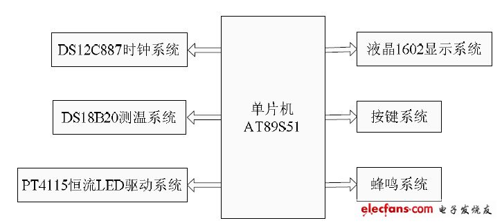
Figure 1 System structure diagram
1.1 MCU main control system
The main control system of this design is implemented by ATMEL's high-performance AT89S51 chip. Its P0 port is connected to a 10K pull-up resistor. P0.0~P0.7 are used as the data interface of DS12C887 and the data interface of LCD 1602. P2.0~P2.3 are respectively connected to the chip select terminal CS, address select input terminal AS, data select terminal DS and read/write input terminal R/W of DS12C887 chip, and P3.2 is connected to its alarm interrupt request output terminal IRQ. P2.5~P2.7 are respectively connected to the enable terminal EN, data/command select terminal RS, and read/write select terminal RW of LCD 1602. P2.4 is used as the buzzer control terminal. P3.0 is used as the signal input terminal of DS18B20. P3.1, P3.4, P3.5, P3.6 and P3.7 are used as S2~S6 key system. P1.1 is used as the output terminal of PWM signal and connected to the DIM terminal of PT4115 chip for PWM dimming control. The system crystal oscillator circuit is composed of 12MHZ crystal oscillator and two 30PF capacitors; the reset circuit is composed of S1 button, 10K resistor and 10uF electrolytic capacitor. The main control system circuit is shown in Figure 2.
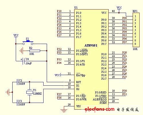
Figure 2 MCU main control system circuit diagram
1.2 Constant current drive system
The LED light source in this design is connected in parallel, and consists of 20 5mm high-brightness low-power LED lamp beads; the voltage drop of each LED lamp bead is about 3.1V, and the working current is about 20mA. From the forward volt-ampere characteristics of white light LED, it can be seen that when the LED terminal voltage exceeds its forward conduction voltage, a small voltage fluctuation will cause a drastic change in the working current, thereby affecting the normal use of the LED. Therefore, the LED should be driven by a constant current. Therefore, this design uses a high-performance PT4115 constant current chip driver. PT4115 is a step-down constant current source chip with a continuous inductive current conduction mode, which can directly convert DC voltage into a stable constant current output; it uses a 6~30V wide voltage input, the output current can reach 1.2A, the conversion efficiency is as high as 97%, and the output current accuracy is ±5%. The chip contains a frequency jitter characteristic, which greatly improves EMI, and has multiple functions such as over-temperature, over-voltage, over-current, and LED open circuit protection. This chip is suitable for the driving circuit of green lighting LED lamps, and has the advantage of a very simple application circuit. The LED constant current driving circuit is shown in Figure 3.
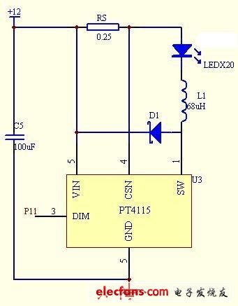
Figure 3 LED constant current drive system circuit diagram
Through the DIM terminal on the PT4115 chip, analog or PWM dimming can be easily performed. Since analog dimming directly changes the size of the current flowing through the LED to achieve brightness adjustment, in addition to the change in brightness, it will also affect the quality of white light, that is, the white light emitted under different currents has color deviation. Therefore, this design adopts the PWM dimming solution. The basic principle of PWM dimming is to keep the LED forward current constant, and by controlling the time ratio of the current on and off, that is, changing the duty cycle of the input pulse signal, the LED will produce brightness changes; and using the visual residual effect of the human eye, when the frequency of the LED brightness change is greater than 120Hz, the human eye will not feel the flicker, but see the average brightness of the LED. The advantage of PWM dimming is that the LED forward current is constant, and the chromaticity of the LED will not change like analog dimming. [page]
The current value calculation formula of PT4115 constant current drive output is:
IOUT =(0.1×D)/ Rs (D is the duty cycle of the square wave signal, Rs is the current limiting resistor.
The LED light source in this design uses 20 low-power white LED lamp beads in parallel, and the rated current of each LED lamp bead is 20mA, so the maximum current IOUT of the PT4115 constant current driver output should be 400mA, so Rs selects a 0.25Ω resistor.
L1 is the ballast inductor, which is selected as 68μH and is used to stabilize the current passing through the LED. D1 is a freewheeling diode, which provides a discharge circuit for the current stored in the inductor L1 when the MOS tube inside the chip is cut off; due to the high frequency operation, D1 uses a Schottky diode SS24 with a small forward voltage drop and fast recovery speed.
The PWM pulse signal is generated by the single-chip microcomputer P1.1, and its high and low levels determine the on and off state of the LED. The overflow interrupt of timer T0 is set to 1/2500 second (ie 400μ S), and every 10 pulses are regarded as a cycle, that is, the frequency is 250HZ. In this way, in every 1/250 second square wave cycle, by changing the output duty cycle of the square wave, the 10-level brightness adjustment of the LED lamp is realized, that is, the LED brightness level is determined by the number of high-level pulses in each cycle. When the number of high-level pulses is 1, the duty cycle is 1/10, the brightness is the lowest, and its dimming principle is shown in Figure 4; when the number of high-level pulses is 10, the duty cycle is 1, and the LED brightness is the highest.
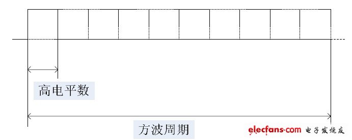
Figure 4 PWM dimming principle diagram
1.3 Clock system
The clock system uses a high-performance DS12C887 clock chip, which is rich in functions and easy to use. It is a high-precision real-time clock chip. It can automatically generate century, year, month, day, hour, minute, second and other time information, has leap year compensation and alarm (timing) functions, and has its own internal lithium battery. When the external power is off, the clock can still be kept accurate, and its internal time information can be maintained for 10 years. After the external system is powered off, the user does not need to reset the time.
The DS12C887 clock chip has two bus working modes, namely Motorola and Intel modes. This design uses the Intel mode, that is, the first pin MOT of the chip is connected to GND. At the same time, the clock system is set to 24-hour mode, and the register storage mode is selected as binary format. P0.0~P0.7 connects its address data multiplexing port AD0~AD7. P2.0~P2.3 are respectively connected to the chip select terminal CS, address selection input terminal AS, read/write input terminal R/W and data selection terminal DS.
P3.2 is connected to the interrupt request output terminal IRQ, which is used to process the alarm interrupt. The clock interface circuit is shown in Figure 5.

Figure 5 Clock system circuit diagram
1.4 LCD display system
The display system uses 1602 character LCD. This LCD can display two lines, each line displays 16 characters; it is small in size, low in energy consumption, and simple to operate; it is suitable for the display requirements of numbers, English letters and special symbols required by this design. The 1602 LCD is controlled by a single-chip microcomputer to display the year, month, day and week on the first line, and the hour, minute, second and ambient temperature on the second line.
The 1602 LCD in this system adopts parallel operation mode. P0.0~P0.7 is connected to its data port DB0~DB7 through a 10K pull-up resistor. P0 port is also connected to the data address port of DS12C887. Since the chip select signals are different, the operation of the corresponding chip will not cause operation conflicts when selected. P2.5~P2.6 are respectively connected to the enable terminal E, read/write selection terminal RW, and data/command selection terminal RS of the 1602 LCD. The third pin is the LCD display contrast adjustment terminal, which is grounded through a 10K sliding rheostat to adjust the display brightness of the LCD. The 15th pin backlight positive pole BLA is grounded through a 10 ohm resistor, and the 16th pin backlight negative pole BLK is grounded. The LCD interface circuit is shown in Figure 6.

Figure 6 LCD system circuit diagram
1.5 Temperature detection system
The temperature detection system uses the digital temperature sensor DS18B20 with a "one-line bus" interface from DALLAS. The sensor has the advantages of miniaturization, low power consumption, and high performance. It can directly convert the temperature into a serial digital signal for processing. The temperature measurement range is -55~125℃, and the highest resolution can reach 0.0625℃. DS18B20 has three pins: positive power supply VCC, negative power supply GND, and signal input and output port DQ. R3 is a 4.7K pull-up resistor, which is used to ensure that the high and low levels are accurately recognized by the single-chip microcomputer and DS18B20 when the single-chip microcomputer communicates with DS18B20. The single-chip microcomputer P3.0 port is connected to the DQ port through R3 to realize the acquisition and processing of temperature data, and it is displayed in real time on the LCD screen. The temperature detection circuit is shown in Figure 7.

Figure 7 Temperature detection circuit diagram
1.6 Buzzer system
The buzzer system is used to generate alarm sounds and key prompt sounds. The P2.4 port of the microcontroller controls the on and off of the PNP transistor 9012 to control the buzzer sound; the delay function is used to control the length of the buzzer alarm sound. The long sound "di" is used for the alarm ringtone, and the short sound "di" is used for the key prompt tone. The buzzer system circuit is shown in Figure 8.

Figure 8 Buzzer system circuit diagram
1.7 Keyboard System
The key control system consists of five keys S2~S5, which are S2 time setting key, S3 value increase key, S4 value decrease key, S5 alarm setting key and S6 brightness adjustment key. S2 is used to select the time calendar and alarm parameters to be adjusted, and is used as the storage confirmation key for the time calendar parameters. S3 and S4 are used to adjust the value of the selected parameter. S5 is used for alarm viewing and storage confirmation key. S6 is used for adjusting the 10-level brightness of the LED light. The key system circuit is shown in Figure 9. [page]

Figure 9 Key system circuit diagram
1.8 Power System
The maximum power of this system is about 1.6W, and it can be powered by batteries or regulated power supplies. Since the system light source is composed of 20 LED lamp beads in parallel, the LED constant current driver chip PT4115 power supply can make the LED lamp work normally within the voltage range of 6~30V. However, the microcontroller power supply system uses a three-terminal voltage regulator chip 7805. The difference between the normal working input voltage and output voltage of this linear voltage regulator chip should be at least higher than 2V. If the difference is too large, it will increase the extra power consumption. Therefore, this system should be powered by 2 4.2V lithium batteries or 9V regulated power supplies. At the same time, the design of the LED constant current drive system in this article is simple and flexible. The drive circuit parameters can be adjusted appropriately according to user needs, which can expand the LED lighting power to a maximum of about 10W.
2 System Software Design
The system control program mainly includes system initialization program, real-time clock chip processing program, temperature sensor chip processing program, LCD display program, keyboard detection and processing program, alarm interrupt and timer PWM generation program.
2.1 System main program
The main program of the system mainly includes the system initialization program (including I/O port initialization, DS12C887 clock chip initialization, LCD 1602 initialization, external interrupt 0 and timer T0 setting), key detection and processing program, clock data reading and processing program, temperature data reading and processing program, LCD display program, alarm judgment and processing program, PWM dimming processing program, etc. The alarm flag Flag_ri is set in the program. Once the alarm time arrives, the clock chip IRQ pin triggers external interrupt 0, and Flag_ri=1 is set when entering the interrupt program, which is used for the judgment and processing of the alarm in the main program.
The main program flow chart of the system is shown in Figure 10.

Figure 10 Main program flow chart
2.2 Key detection and processing procedures
The key control system consists of five keys, S2~S6, which are S2 time setting key, S3 value increase key, S4 value decrease key, S5 alarm setting key and S6 brightness adjustment key. S2 is used to select the clock and alarm parameters that need to be adjusted. According to the number of times S2 is pressed, select the second, minute, hour, week, day, month and year in turn. The cursor flashes below the selected parameter on the LCD screen. Then press S3 or S4 to adjust the value of the selected parameter. When S2 is pressed 8 times, the selection function is exited and the current data is saved to the clock chip. S5 is used to view and set the alarm time; when S5 is pressed for the first time, the second line of the 1602 LCD screen displays the set alarm time; the alarm time can be reset through S2, S3 and S4; press again to exit the alarm viewing function and save the currently set alarm parameters to the clock chip. At the same time, S3 and S4 can also be used independently as the cancel key when the alarm is generated and the off key of the LED light. S6 can adjust the brightness of LED light in 10 levels. Each time it is pressed, the brightness of LED light increases by one level. When the brightness reaches the maximum, pressing it again turns off the LED light. Each time a key is pressed, the buzzer will give a short beep. The key detection and processing flow chart is shown in Figure 11.

Figure 11 Key detection and processing flow chart
2.3 Alarm interrupt procedure
When the system reaches the set alarm time, the IRQ pin output of the DS12C887 clock chip changes from high level to low level, which is used as the application input of the INT0 interrupt of the P3.2 port of the microcontroller, and the IRQ pin output can be cleared by reading the C register of the DS12C887 chip. Therefore, the external interrupt INT0 is set to a negative edge trigger interrupt, and the alarm flag Flag_ri is set. When the alarm time arrives, Flag_ri=1 is set for the alarm alarm processing in the main program. The alarm interrupt program is shown in Figure 12. [page]

Figure 12 Alarm interrupt flow chart
2.4 Timer interrupt program
To generate a PWM signal to adjust the brightness of the LED light, timer T0 is set to work mode 0, that is, 13-bit counter timing, and the maximum load value is 213=8192. Because the system crystal oscillator uses 12MHz, the assignment makes TH0=(8192-400)/32 and TL0=(8192-400)%32, which can achieve a 400μS timing interrupt. 10 interrupts (i.e. 4mS) as a cycle, and the PWM pulse signal is generated by adjusting the duty cycle of the microcontroller P1.1 (the control port name is defined as LED_PWM) output in each cycle to control the PT4115 constant current driver chip to achieve 10 levels of brightness adjustment of the LED light.
The program is set to count the number of T0 interrupts (defined as T0_num) to determine whether a cycle has arrived; at the same time, the number of high-level pulses (defined as scale value, set by the number of times the dimming key S6 is pressed) is determined to achieve different brightness levels. In the timer T0 interrupt service program, first, T0 is reloaded with the initial value of 400μ S; the number of timer interrupts T0_num is increased by 1 to determine whether a square wave cycle has arrived. If it has arrived, T0_num is reset to zero and the output level of P1.1 port is set high (ie LED_PWM=1); if a square wave cycle has not arrived, it is compared with the brightness level scale value to determine whether the number of high-level pulses scale has arrived. If it has arrived, the output level of P1.1 port is set low (ie LED_PWM=0), otherwise the output level of P1.1 port continues to be kept high (ie LED_PWM=1); then the interrupt returns and waits for the next timing interrupt.
In this way, the P1.1 port generates the required PWM dimming signal. The timer generates PWM flow chart as shown in Figure 13.
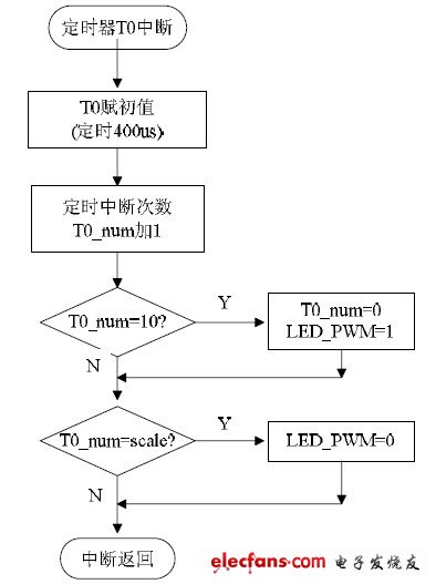
Figure 13 Timer generates PWM flow chart
3 Experimental Results
According to the above design scheme, this paper made this multifunctional LED desk lamp based on PWM dimming. After debugging, the system runs stably and reliably, and can basically meet the requirements of family life. When the system is working, the minimum power (i.e. LED off state) is 0.28W; the maximum power (i.e. LED highest brightness state) is about 1.52W; at the same time, the LCD displays time, calendar and temperature data accurately, and the alarm function is stable. The actual photo is shown in Figure 14.

Figure 14 Actual photo
Previous article:Classroom lighting energy-saving control system based on STC89C51
Next article:Design of signal generator based on AD9851
Recommended ReadingLatest update time:2024-11-16 19:56


- Popular Resources
- Popular amplifiers
 Professor at Beihang University, dedicated to promoting microcontrollers and embedded systems for over 20 years.
- Innolux's intelligent steer-by-wire solution makes cars smarter and safer
- 8051 MCU - Parity Check
- How to efficiently balance the sensitivity of tactile sensing interfaces
- What should I do if the servo motor shakes? What causes the servo motor to shake quickly?
- 【Brushless Motor】Analysis of three-phase BLDC motor and sharing of two popular development boards
- Midea Industrial Technology's subsidiaries Clou Electronics and Hekang New Energy jointly appeared at the Munich Battery Energy Storage Exhibition and Solar Energy Exhibition
- Guoxin Sichen | Application of ferroelectric memory PB85RS2MC in power battery management, with a capacity of 2M
- Analysis of common faults of frequency converter
- In a head-on competition with Qualcomm, what kind of cockpit products has Intel come up with?
- Dalian Rongke's all-vanadium liquid flow battery energy storage equipment industrialization project has entered the sprint stage before production
- Allegro MicroSystems Introduces Advanced Magnetic and Inductive Position Sensing Solutions at Electronica 2024
- Car key in the left hand, liveness detection radar in the right hand, UWB is imperative for cars!
- After a decade of rapid development, domestic CIS has entered the market
- Aegis Dagger Battery + Thor EM-i Super Hybrid, Geely New Energy has thrown out two "king bombs"
- A brief discussion on functional safety - fault, error, and failure
- In the smart car 2.0 cycle, these core industry chains are facing major opportunities!
- The United States and Japan are developing new batteries. CATL faces challenges? How should China's new energy battery industry respond?
- Murata launches high-precision 6-axis inertial sensor for automobiles
- Ford patents pre-charge alarm to help save costs and respond to emergencies
- New real-time microcontroller system from Texas Instruments enables smarter processing in automotive and industrial applications
- Conversion between CC2640R2F projects
- Pengfeng Technology RVBoards-Nezha (RISC-V SBC) Allwinner Development Board Introduction Part 3
- Cadence Certus Closure Solution is a new generation chip-level convergence solution. Welcome to learn more!
- What is the progress of domestic NPU chips?
- How is JTAG used for chip testing?
- Talk about downloading the DSP28335 register manual
- [Gizwits Gokit3 Review] Device Access-Step 1: Create a New Solution Project
- Circuit Diagram
- Apple faces ultimatum! EU finalizes: Type-C interface will be fully adopted in 2024
- Navi10 Macro Keyboard with KB2040 and KMK CircuitPython Keyboard Firmware

 西门子S7-12001500 PLC SCL语言编程从入门到精通 (北岛李工)


 京公网安备 11010802033920号