Since the emergence of photolithography technology, the size of integrated circuits (ICs) has continued to shrink in line with Moore's Law. Today, with the mass production of 5 nanometers, ICs can be said to have shrunk by a million times! This achievement was not achieved overnight, but is the result of years of hard work by semiconductor R&D personnel and engineers. In the 111th Knowledge Feast of the Academia Sinica, Academician Lin Benjian shared how photolithography technology has been used to shrink the size of semiconductor components to the limit.
With the development of integrated circuits (ICs) and semiconductor manufacturing processes, 3C products such as smartphones and tablets are becoming smaller and smaller, faster and faster, and more and more powerful. This is because semiconductor technology is making ICs smaller and smaller, and the number of components that can be put into 3C products is increasing, so naturally more things can be done and efficiency is increased.
The key technology to making ICs smaller and smaller is optical lithography. In simple terms, optical lithography is the technology of "printing" the component materials on the semiconductor wafer according to the required position when making components. The finer the pattern that can be printed, the smaller the component can be made.
One of the key indicators for measuring component size is the "gate length of the transistor", which is directly related to the speed of the IC. For field-effect transistors, the smaller the gate length, the less time the current takes to pass through the transistor drain and source.
If we want to express the degree of component miniaturization, another key indicator is line width and pitch. Usually, the pitch between metal layer lines is used as a reference. The smaller the pitch, the smaller the line width and the higher the degree of component miniaturization.
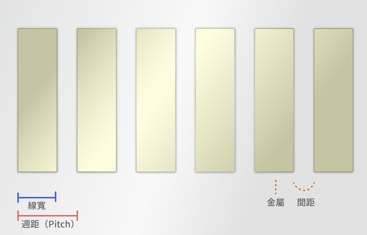
Schematic diagram of line width and circumference. The circumference is the line width plus the distance between lines, which can represent the scale of the periodic arrangement of metal wires.
Now we have reached the single-digit nanometer generation (such as 7nm or 5nm process), and these numbers have gradually evolved into generational symbols. Although the smaller the IC, the better, the new generation of process may represent other comprehensive advantages such as fast computing, high density, and low price.
How much has IC shrunk so far? Here's a concept. If we consider each generation as the actual size, since the advent of photolithography in the 1980s, the line width has dropped from 5,000 nanometers to 5 nanometers today, and is even heading towards 3 nanometers. The line width keeps shrinking, with each generation shrinking by about 0.7 times the previous generation, and 5 nanometers is the 21st generation. After "passing down from generation to generation", the line width has shrunk by 1,000 times, which means that the number of components that can be placed in the same area is as high as 1 million times the original number!
Photolithography technology is like magic, reducing line width step by step, relying on the hard work of researchers over the years. Academician Lin Benjian listed the key improvements and challenges in the popular science lecture "Photolithography Technology Reduces IC by Millions of Times".
How to shrink IC? Pursuing the minimum line width
Let’s start with the core optical resolution formula:
Half Pitch = k1λ/sinθ
Half-circle distance: the width of a line plus the spacing between lines multiplied by 0.5. When the exposure resolution is high, the smaller the half-circle distance can be, the smaller the line width.
k1: Coefficient, related to the manufacturing process, the key to reducing the half-circle pitch, which is the goal that all semiconductor engineers strive to reduce.
λ: The wavelength of the light source in the lithography process has been reduced from 436 nanometers at the beginning to 13.5 nanometers.
sinθ: It is related to the angle at which the lens focuses light onto the imaging surface and is basically determined by the lens.
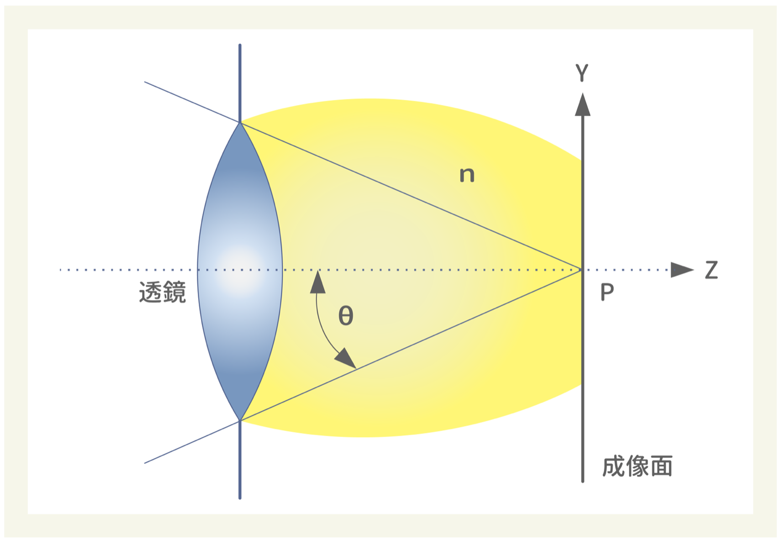
Since the wavelength of light changes in different media, when considering how to increase resolution, the medium (refractive index n) of the lens and the imaging surface (wafer) can be taken into consideration, and λ can be changed to λ0/n, where λ0 is the vacuum wavelength.
Half Pitch = k1λ0/n sinθ
Therefore, the efforts to increase exposure resolution (half-circle distance↓) are as follows: increase sinθ, reduce λ0, reduce k1, and increase n.
On the other hand, in order to allow the lithography process to have a large enough exposure clarity range, the larger the lens imaging depth of field (DOF) number, the better (Note). However, the side effect of a larger depth of field is that the half-circle distance will also become larger. Therefore, process improvements must consider the balance between the two or sacrifice each other.
Adding sinθ: A huge and complex lens
Sinθ is related to the focusing angle of the lens. The value is determined by the lens. The larger the sinθ, the higher the resolution. The photolithography lens is not as simple as an ordinary camera or telescope. Instead, it is composed of a large number of lenses of different sizes, thicknesses and curvatures, which are carefully stacked after precise calculation (see the figure below).
This lens is extremely sophisticated. Lin Benjian revealed: "A lens costing $60 million is not uncommon, and $100 million is possible." The lens is complex, large, and expensive in order to get sinθ as close to the extreme value as possible, which is 1. "The current lens can achieve a sinθ value of 0.93, which is very hard work."
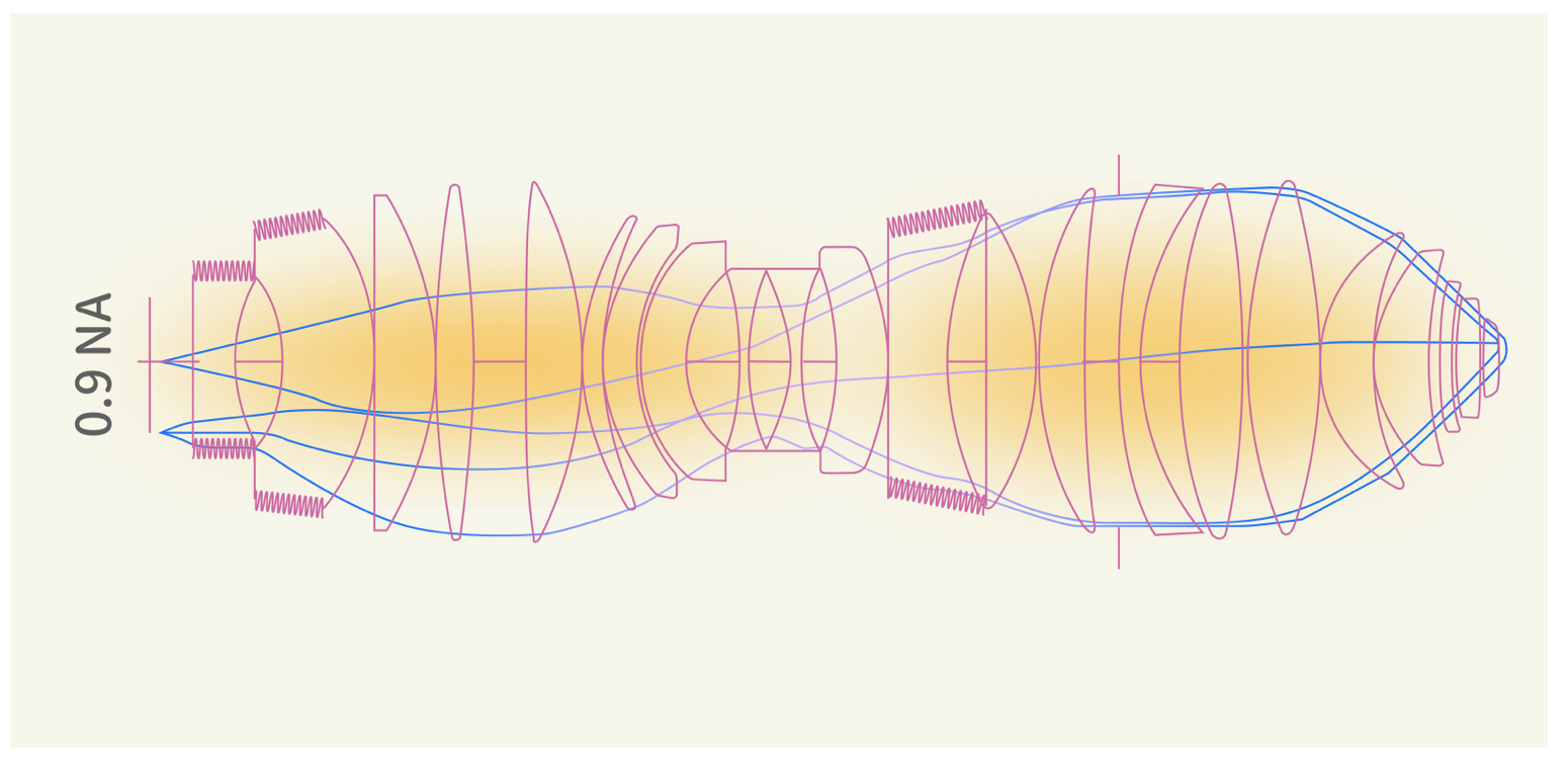
The lens design of the lithography machine is quite complex. Lin Benjian mentioned that the industry is currently trying to increase the sinθ value to 0.93. In the figure, NA = n. sinθ = 0.9, and the refractive index of air n is about 1, so the sinθ of the lens is 0.9. When the lens module is actually used, it will stand vertically to the ground (as shown below).
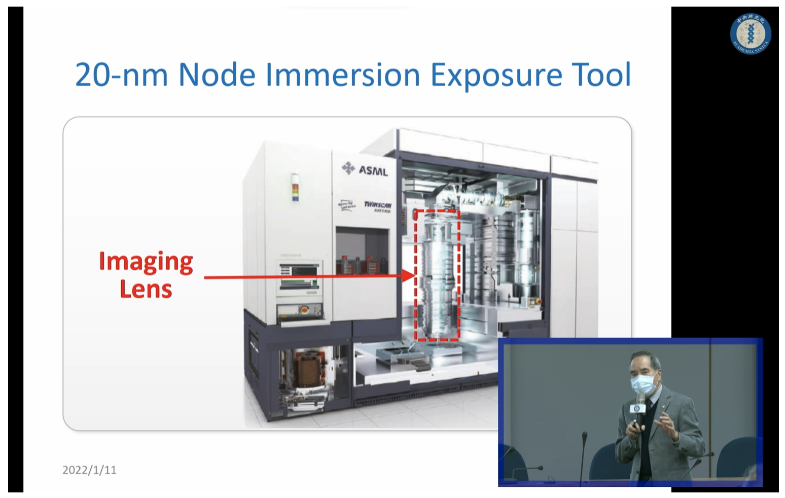
Lin Benjian's lithography machine lens module is very large and heavy, so heavy that a crane must be used to move it.
Shortening wavelengths: precise matching of materials and lenses
The second method is to shorten the wavelength. Although different wavelengths can be obtained by changing the light source, different wavelengths of light will be refracted in different directions after passing through the lens, so the lens material must also be changed. Lin Benjian said that as the wavelength becomes shorter and shorter, "the lens materials we can choose from become fewer and fewer, and in the end there are only two or three that can be used."
It became increasingly difficult to adjust the bandwidth of the light source using a few materials. Later, people switched to choosing a single suitable material and narrowing the bandwidth as much as possible for the wavelength that suits this material. Lin Benjian said: "Even the bandwidth of the laser is not narrow enough. Now the bandwidth has been narrowed to an unimaginable degree."
Another way to solve the problem is to add a reflector to the lens composition, which is called a catadioptric system. Regardless of the wavelength of light, the angle of incidence and the angle of reflection when encountering the mirror are equal. If some reflective mirrors can be used to replace the lens, the tolerance to the light wave bandwidth can be increased.
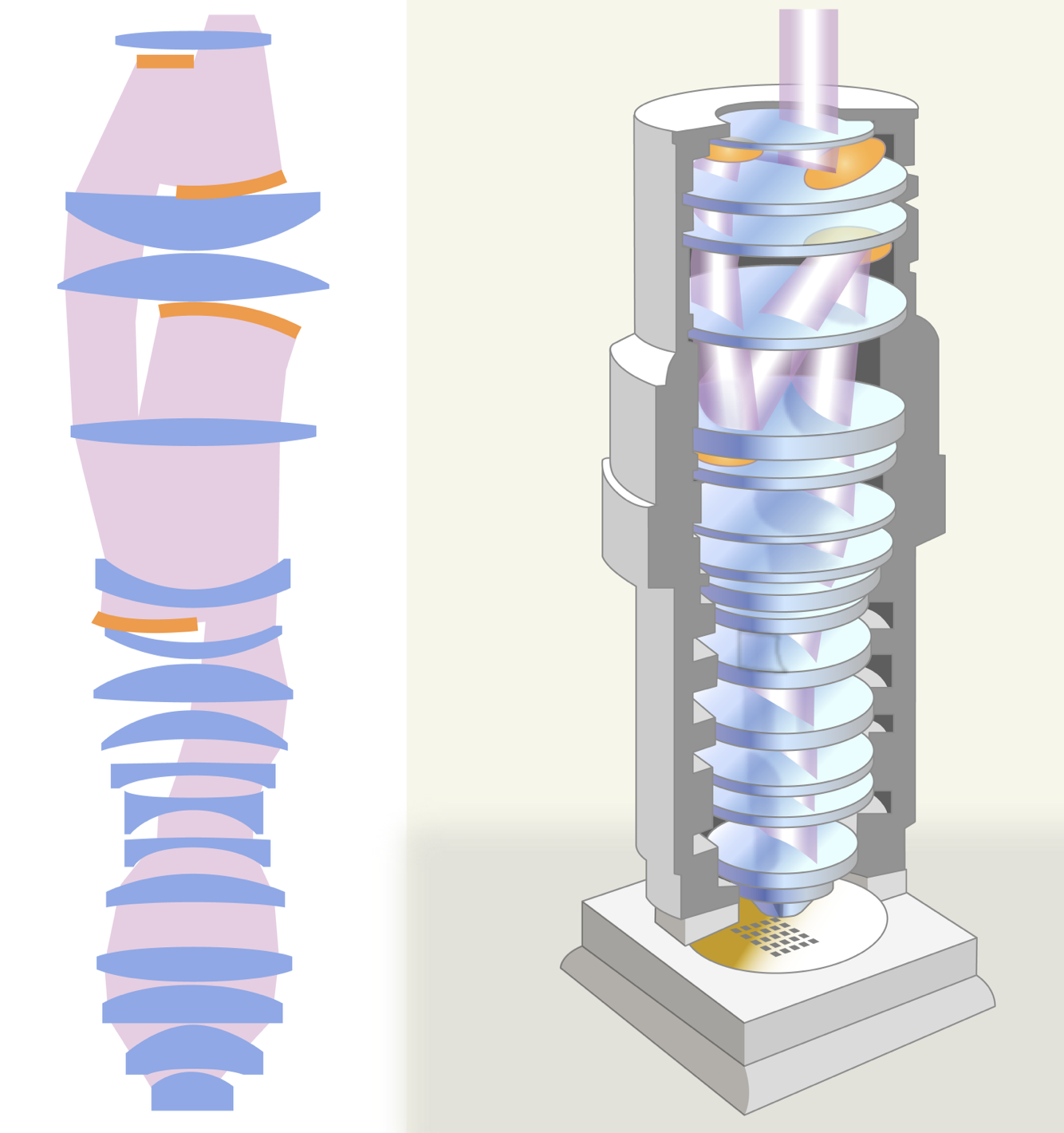
The exposure lens module of the 193 nanometer wavelength light source shows the addition of a reflector to the lens assembly.
Later, when the wavelength reached 13.5 nanometers (extreme ultraviolet light, EUV), even the entire set of lenses had to use reflectors, which is called a fully reflective optical system. Please refer to the ASML demonstration video below. Lin Benjian said that the fully reflective mirror system must be designed to allow the light beams to avoid each other so that the lenses do not block the light. In addition, compared with the lens penetration angle, the error tolerance of the mirror reflection angle is lower, and the mirror angle must be very, very accurate. All of the above increase the difficulty of design.
Changes in exposure wavelength will also affect the exposure photoresist. All properties of the photoresist material, from chemical properties, transmittance to sensitivity, must be adjusted as the exposure wavelength changes. "This is a huge project, and the photosensitivity is very important. It is the key to saving manufacturing costs." Lin Benjian said.
It is worth mentioning that the photosensitivity of photoresist materials is very important in the history of miniaturized ICs. In the 1980s, CG Willson and H. Iro, then at IBM, first proposed a method to chemically amplify the photosensitivity of photoresists, increasing the photosensitivity by 10 to 100 times and greatly increasing exposure efficiency. This major invention earned CG Willson the Japan Prize in 2013, but unfortunately Dr. H. Iro had passed away at the time and could not receive the award together.
Reducing k1: Resolution Enhancement Technology (RET)
The key to improving resolution is to lower k1. Lin Benjian said: "You don't have to buy expensive lenses, and you don't have to choose new wavelengths that require a lot of research and development. As long as you can use your intelligence and creativity to lower k1."
The first is "anti-vibration", just like turning on the anti-shake function when taking a photo. When the wafer is exposed, try to reduce the relative vibration between the wafer and the mask, so that the exposure pattern is more accurate and the resolution lost due to vibration is restored. The second is "reducing useless reflections". When exposing, many surfaces will produce unnecessary reflections, and we need to try to eliminate them. Lin Benjian said that by improving the above two items, k1 can reach the 0.65 level.
To improve the resolution, two-beam imaging methods can be used, including Off-Axis Illumination (OAI) and Phase Shift Mask (PSM).
Previous article:Flexible PCB Technology Analysis
Next article:Application is king, Yuefang Technology reveals that the underlying logic of chip product definition reflects future planning
- Popular Resources
- Popular amplifiers
- ASML provides update on market opportunities at 2024 Investor Day
- It is reported that memory manufacturers are considering using flux-free bonding for HBM4 to further reduce the gap between layers
- Intel China officially releases 2023-2024 Corporate Social Responsibility Report
- Mouser Electronics and Analog Devices Launch New E-Book
- AMD launches second-generation Versal Premium series: FPGA industry's first to support CXL 3.1 and PCIe Gen 6
- SEMI: Global silicon wafer shipment area increased by 6.8% year-on-year and 5.9% month-on-month in 2024Q3
- TSMC's 5nm and 3nm supply reaches "100% utilization" showing its dominance in the market
- LG Display successfully develops world's first stretchable display that can be expanded by 50%
- Infineon's revenue and profit both increased in the fourth quarter of fiscal year 2024; market weakness in fiscal year 2025 lowered expectations
- LED chemical incompatibility test to see which chemicals LEDs can be used with
- Application of ARM9 hardware coprocessor on WinCE embedded motherboard
- What are the key points for selecting rotor flowmeter?
- LM317 high power charger circuit
- A brief analysis of Embest's application and development of embedded medical devices
- Single-phase RC protection circuit
- stm32 PVD programmable voltage monitor
- Introduction and measurement of edge trigger and level trigger of 51 single chip microcomputer
- Improved design of Linux system software shell protection technology
- What to do if the ABB robot protection device stops
- Detailed explanation of intelligent car body perception system
- How to solve the problem that the servo drive is not enabled
- Why does the servo drive not power on?
- What point should I connect to when the servo is turned on?
- How to turn on the internal enable of Panasonic servo drive?
- What is the rigidity setting of Panasonic servo drive?
- How to change the inertia ratio of Panasonic servo drive
- What is the inertia ratio of the servo motor?
- Is it better for the motor to have a large or small moment of inertia?
- What is the difference between low inertia and high inertia of servo motors?
- diode
- 【GD32L233C-START Review】WS2812B Display Driver
- Diwen 86 box data sharing
- Competition-risk phenomenon when using Huada MCU ports
- Why is your MOSFET getting so hot?
- Thank you for being there - Tribute to my love
- 【Bluesun AB32VG1 RISC-V Evaluation Board】Development of example programs
- 2nd day to go!! Pre-registration for the prize live broadcast | ON Semiconductor image sensors help the automotive, machine vision and artificial intelligence fields....
- 【AT-START-F425 Review】USB to CAN Preview Post
- Abnormal sound from the front transformer of the power factor circuit


 HA7-5102-7


 京公网安备 11010802033920号