This paper first introduces how to use automated synthesis tools to optimize HDTV chip design in the coding and synthesis stages. Since the quality of Verilog code will directly affect the results of synthesis, the synthesis requirements should be taken into account in the code design stage. Secondly, the characteristics and structure of the HDTV chip are introduced, focusing on the difficulties and solutions caused by the complex structure of the HDTV chip. Finally, it introduces how to use the synthesis tool Design Compiler to optimize the design of the HDTV chip and reduce the delay from -0.94 to 0.11.
VerilogHDL comprehensive design
1 Clock arrangement
Choose a rising edge triggered single clock signal and try not to use a mixed triggered clock signal. Because the clock period is a key issue in the timing analysis process, it also affects the clock frequency. Using a simple clock structure is conducive to the analysis and retention of the clock signal, avoiding adding a buffer to the clock signal, and also conducive to obtaining better synthesis results. Figure 1 shows the rising edge triggered single clock signal structure.

Try to avoid using gated clocks. Clock gating circuits are usually related to process and timing. Incorrect timing relationships can lead to incorrect clocks and pulse interference. Clock skew can lead to confusion in hold time, as shown in Figure 2. In addition, gated clocks can reduce the testability of the design.

At the same time, avoid using internal parasitic clocks and parasitic resets. Parasitic clocks cannot be used as part of the scan chain, so the testability of the design will be reduced and the difficulty of comprehensive constraint design will increase. Only some low-power designs require gated clocks. In the top-level module, pay attention to making the clock or reset circuit as a discrete module.
2 Comprehensive code
Using synthesizable code can improve the testability of the circuit, simplify static timing analysis, and make the gate-level circuit and the original register-level code functionally consistent.
Use registers instead of combinational logic feedback and avoid using latches. Registers are favored by sequential logic because they maintain consistency and synthesis correctness. Use reset signals to initialize register signals in your design. Do not use initial statements in Verilog to initialize signals.
In each always block, specify a complete list of sensitive signals. If you do not specify a complete list of sensitive signals, the results of the behavioral front-end synthesis and back-end synthesis netlist will not match. The synthesis tool will give a warning when elaborate the design. If you add extra sensitive signals, the simulation speed will be reduced. In addition, pay attention to the problem of blocking assignment and non-blocking assignment. Blocking assignment is generally used in sequential circuits.
The case statement is equivalent to a single-layer multiplexer; the if-then-else statement is equivalent to a stacked combinational multiplexer. A single multiplexer is faster, so it is usually recommended to use the case statement. Avoid using full-case and parallel_case, which will cause differences in the interpretation of the code during simulation and synthesis.
The code for writing sequential logic should include a state machine and a sequential process. Use the assign statement outside the process to generate complex internal intermediate variables to improve the readability of the code. Use the define statement to define the state vector. Putting finite state machines and non-finite state machines in different modules is conducive to synthesis.
Do not use any delay constants in the RTL code. Delays will not only cause inaccuracies in some environments, but will also make simulation and synthesis results inconsistent and disrupt RTL simulator code optimization.
3 Code Division
In order to obtain better synthesis results, faster synthesis speed, and use simple synthesis strategies to meet timing requirements, it is recommended to use the following synthesis partitioning technology.
● All modules use register outputs. All output signals should be recorded for each submodule of the design, which can simplify the synthesis process and predict the output drive capability and input delay.
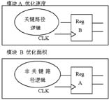
● Put local related combinational logic into the same module, and put designs with different goals into different modules. For example, during the synthesis process, put the critical path logic that needs to be optimized for area and speed into two separate modules, as shown in Figure 3.

● The main criteria for dividing the synthesis time are logic function, design goal, timing and area requirements. Accurate timing calculation and appropriate constraints have a much greater impact on the synthesis time than circuit size. Putting the circuit logic of the same design goal together will also reduce the synthesis time, while too many design constraints will increase the synthesis time. The key to reducing the synthesis time is to make an accurate time budget before designing, and make the macro modules of the design meet the budget requirements, then write the synthesis constraints to meet the budget, and finally use the commands of the synthesis tool to implement the constraints.
● Avoid timing anomalies. Timing anomalies mainly include multicycle path and false path. If multicycle path must be used in the design, the start and end points should be recorded to ensure validity at the chip level. Try to avoid using asynchronous logic, which will make the correctness and verification of the design difficult.
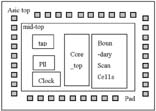
● Pay attention to the placement of glue modules. Place the top-level connection modules into the bottom-level modules, and make sure the top-level contains I/O pins and clock generators, as shown in Figure 4.

Features of HDTV chips
The designed chip uses a large number of different types of RAM, including 1 single-port RAM, 2 dual-port RAMs, 3 ROMs and 20 register stacks.
The chip requires multiple clock signals (27MHz, 74MHz, 150MHz) and selects the clock through the clock mux. The 27MHz clock is used for the PCI bus clock in the DMA module. At the same time, it and the 74MHz clock determine whether it is HDTV mode or SDTV mode decoding through mode selection. The Pll core clock frequency is 13.5MHz. The Pll input clock is multiplied by 11 to generate a 148.5MHz clock. The Pll clock is also used for testing. In addition, there are 6 output clocks that drive external chips, namely PCI clock, video clock, 2 SDRAM clocks and 2 SRAM clocks.
In order to obtain a high test coverage, this design uses a variety of test methods, such as scan chain, boundary scan and memory built-in self-test (BIST). Most modules in this design use the BIST method to achieve the test purpose, and the Mentor Mbistarchitect tool is used to automatically insert the BIST code. The other parts use the Mentor Jtag tool to implement boundary scan and insert JTAG code.
The chip is connected to high-speed SDRAM and SRAM outside, and each module includes 4 RAMs. The HDTV chip mainly uses the sdr_ssr_sel signal to achieve the conversion between the two environments.
As shown in FIG5 , the structural design of the HDTV chip is complex and the chip is mainly divided into three layers, among which core_top is not dependent on the process and its main function is to complete the decoding of the HDTV code stream.

As mentioned above, these characteristics of the chip put forward very high requirements for the back-end layout and routing. The synthesis results will directly affect the layout and routing (floor planning), so the synthesis method is very important.
Comprehensive Solution
1 Preliminary Synthesis
First, perform a rough top-down synthesis on the design and check the synthesis result report. Set basic Design Rules and Design Constraints according to the PDK data. Including Setting Design Environment (Fanout load, Output load, Input drive impedance) and Setting Design Constraints (Design Rules Constraints (max_transition, max_fanout, max_capacitance), Timing Constraint (max_delay, min_delay), Area Constraint). The delay results after preliminary synthesis are shown in Table 1.

The slack=-0.94 given in Table 1 is the result without considering wireload, so it still needs a lot of improvement.
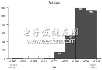
Figure 6 shows the path slack distribution result obtained by using design_vision to count the critical paths after synthesis.

According to the above statistical results, the core-top module has the most critical paths that do not meet the timing requirements, so it is necessary to optimize the core-top module separately to obtain better synthesis results. First, set the Design Environment and Design Rules, and then optimize the delay.
Design Compiler optimizes the timing of the design based on the specified delay constraints. The constraints that affect the delay include clock, input and output delays, external loads, input cell drive capabilities, operating environment, and line load models. The specific methods to solve the delay problem are as follows.
● Use the set_false_path command. In a design with more than two clocks, set a false path between unrelated clocks, otherwise it will waste longer running time and higher memory usage.
● Use the ungroup command to split the underlying modules.
● Use the set_critical_range command to define the optimization range of the critical path.
● Use the set_cost_priority-delay command to set the delay priority higher than the design constraint priority.
● Use the set_ultra_optimization command to compile with an algorithm that calls logic replication and gate mapping.
● The Compile incremental command improves the parts of the design that do not meet the constraints and retains the parts that meet the constraints based on the original synthesis.
● In the compile-map_effort-high command, -high takes longer to compile than -medium and -low, but can produce better synthesis results. This setting can make the critical path synthesized again.
3. Comprehensive results
Figure 7 shows the results of three-step delay optimization, and the specific steps for implementation are as follows.
First, find out the cause of the delay based on the report. According to the report, set the three main clocks to false_path, set multicycle according to the design of the front-end coding stage, and add the following constraints to generate a new report.
Ungroup
Set_critical_range 5
Set_cost_priority -delay
Set_ultra_optimization
Compile incremental
By setting the error path and multiple cycles, the new report shows that the path slack is reduced to -0.50.
Then, use the compile-map_effort high command. According to the report path slack="-0".36, the result needs further optimization.
From the report, we can see that the paths that do not meet the slack requirement are mainly concentrated in the clock signal ve_clk in the video module, pci_clk in the PCI module, and sdr_clk0, sdr_clk1, ssr_clk0 and ssr_clk1 in the RAM module, so we need to add false_path to the above paths. The video_mode_reg module is a module that stores state values. It will not change after writing, so it is also set to false_path. The final result path slack="0".11 meets the requirements.
If the slack is generated by two modules rather than a problem within the module, you can also use the ungroup command to split it. The slack in this result is generated by the ve_mem module, but the slack in the result has met the requirements and will be improved after backend processing.
Conclusion
This paper proposes a solution for HDTV chips from two aspects: coding and synthesis. The design is synthesized by using Synopsys's Design Compiler and the top-down method. The results show that the synthesis scheme meets the synthesis goal well and the effect is obvious.
Previous article:Various PCB design oversights and countermeasures
Next article:Substrate Design Considerations
- Popular Resources
- Popular amplifiers
- Molex leverages SAP solutions to drive smart supply chain collaboration
- Pickering Launches New Future-Proof PXIe Single-Slot Controller for High-Performance Test and Measurement Applications
- CGD and Qorvo to jointly revolutionize motor control solutions
- Advanced gameplay, Harting takes your PCB board connection to a new level!
- Nidec Intelligent Motion is the first to launch an electric clutch ECU for two-wheeled vehicles
- Bosch and Tsinghua University renew cooperation agreement on artificial intelligence research to jointly promote the development of artificial intelligence in the industrial field
- GigaDevice unveils new MCU products, deeply unlocking industrial application scenarios with diversified products and solutions
- Advantech: Investing in Edge AI Innovation to Drive an Intelligent Future
- CGD and QORVO will revolutionize motor control solutions
- Innolux's intelligent steer-by-wire solution makes cars smarter and safer
- 8051 MCU - Parity Check
- How to efficiently balance the sensitivity of tactile sensing interfaces
- What should I do if the servo motor shakes? What causes the servo motor to shake quickly?
- 【Brushless Motor】Analysis of three-phase BLDC motor and sharing of two popular development boards
- Midea Industrial Technology's subsidiaries Clou Electronics and Hekang New Energy jointly appeared at the Munich Battery Energy Storage Exhibition and Solar Energy Exhibition
- Guoxin Sichen | Application of ferroelectric memory PB85RS2MC in power battery management, with a capacity of 2M
- Analysis of common faults of frequency converter
- In a head-on competition with Qualcomm, what kind of cockpit products has Intel come up with?
- Dalian Rongke's all-vanadium liquid flow battery energy storage equipment industrialization project has entered the sprint stage before production
- Allegro MicroSystems Introduces Advanced Magnetic and Inductive Position Sensing Solutions at Electronica 2024
- Car key in the left hand, liveness detection radar in the right hand, UWB is imperative for cars!
- After a decade of rapid development, domestic CIS has entered the market
- Aegis Dagger Battery + Thor EM-i Super Hybrid, Geely New Energy has thrown out two "king bombs"
- A brief discussion on functional safety - fault, error, and failure
- In the smart car 2.0 cycle, these core industry chains are facing major opportunities!
- The United States and Japan are developing new batteries. CATL faces challenges? How should China's new energy battery industry respond?
- Murata launches high-precision 6-axis inertial sensor for automobiles
- Ford patents pre-charge alarm to help save costs and respond to emergencies
- New real-time microcontroller system from Texas Instruments enables smarter processing in automotive and industrial applications
- [NUCLEO-WL55JC2 Review] + Development environment establishment and data preparation
- Xiaodanta teaches you the difference between a handheld radio amplifier and a repeater
- Why does the output voltage of the transistor voltage regulator circuit equal the base voltage minus VBE?
- iTOP3399 development board Android application development environment construction - installation of AndroidStudio (I)
- From acquiring ThreadX to making ThreadX open source, where will Microsoft go next? And how will other RTOS companies respond?
- Intelligent RV control system
- 360° Lid Detection using LSM6DSO
- WIFI6 Explained
- Control battery output and prevent battery reverse connection
- 【NXP Rapid IoT Review】 + Kit Modification-External Lithium Battery (Link)

 HDTV1080p H.264-AVC Encoder Chip Design and Performance Analysis
 ADV7623,pdf,datasheet(HDMI 1.4


 京公网安备 11010802033920号