In this article, I will provide an in-depth look at the different aspects of buck, boost, and buck-boost topologies.
Buck Converter
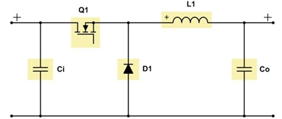
Figure 1 is a schematic diagram of a non-synchronous buck converter. A buck converter steps down its input voltage to a lower output voltage. When switch Q1 turns on, energy is transferred to the output.
Figure 1: Schematic of a nonsynchronous buck converter
Formula 1 calculates the duty cycle:
Equation 2 calculates the maximum metal oxide semiconductor field effect transistor (MOSFET) stress:
Equation 3 gives the maximum diode stress:
Where Vin is the input voltage, Vout is the output voltage, and Vf is the diode forward voltage.
The greater the difference between the input voltage and the output voltage, the more efficient the buck converter is compared to a linear regulator or a low dropout regulator (LDO).
Although the buck converter has a pulsed current at the input, the output current is continuous due to the inductor-capacitor (LC) filter at the output of the converter. As a result, the voltage ripple reflected to the input will be larger than the ripple at the output.
Synchronous rectifiers are recommended for buck converters with small duty cycles and output currents greater than 3 A. If your power supply requires output currents greater than 30 A, multiphase or interleaved power stages are recommended because this minimizes component stress, spreads the generated heat among multiple power stages, and reduces reflected ripple at the converter input.
The duty cycle is limited when using N-FETs because the bootstrap capacitor needs to be recharged at every switching cycle. In this case, the maximum duty cycle is in the range of 95-99%.
Buck converters generally have good dynamic characteristics because they are a forward topology. The achievable bandwidth depends on the quality of the error amplifier and the chosen switching frequency.
Figures 2 to 7 show the voltage and current waveforms of the FET, diode, and inductor in a nonsynchronous buck converter in continuous conduction mode (CCM).

Boost Converter
A boost converter steps up its input voltage to a larger output voltage. When switch Q1 is not conducting, energy is transferred to the output. Figure 8 is a schematic diagram of a non-synchronous boost converter.
Figure 8: Nonsynchronous boost converter schematic
Formula 4 calculates the duty cycle:
Equation 5 calculates the maximum MOSFET stress:
Equation 6 gives the maximum diode stress:
Where Vin is the input voltage, Vout is the output voltage, and Vf is the diode forward voltage.
With a boost converter, a pulsed output current is seen because the LC filter is placed at the input. Therefore, the input current is continuous and the output voltage ripple is greater than the input voltage ripple.
When designing a boost converter, it is important to know that there is a permanent connection from the input to the output, even when the converter is not switching. Precautions must be taken to protect against a possible short-circuit event at the output.
For output currents greater than 4 A, the diodes should be replaced with synchronous rectifiers. If the power supply needs to provide output currents greater than 10 A, a multi-phase or interleaved power stage approach is strongly recommended.
When operating in CCM, the dynamic performance of the boost converter is limited by the right half plane zero (RHPZ) of its transfer function. Since the RHPZ cannot be compensated, the achievable bandwidth will typically be less than one-fifth to one-tenth the RHPZ frequency. See Equation 7:
Where Vout is the output voltage, D is the duty cycle, Iout is the output current, and L1 is the inductor of the boost converter.
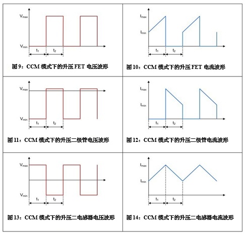
Figures 9 to 14 show the voltage and current waveforms of the FET, diode, and inductor in a nonsynchronous boost converter in CCM mode.

Buck-Boost Converter
A buck-boost converter is a combination of a buck and a boost power stage that share the same inductor. See Figure 15.
Figure 15: Schematic diagram of a two-switch buck-boost converter
The buck-boost topology is useful because the input voltage can be smaller, larger, or the same as the output voltage, while the output power required is greater than 50W.
For output powers less than 50W, the single-ended primary inductor converter (SEPIC) is a more cost-effective option because it uses fewer components.
The buck-boost converter operates in buck mode when the input voltage is greater than the output voltage and in boost mode when the input voltage is less than the output voltage. When the converter operates in the transfer region where the input voltage is within the output voltage range, there are two concepts to handle these situations: either the buck and boost stages are active at the same time, or the switching cycle alternates between the buck and boost stages, each typically running at half the normal switching frequency. The second concept can induce subharmonic noise at the output, and the output voltage accuracy may not be as precise compared to regular buck or boost operation, but the converter will be more efficient compared to the first concept.
The buck-boost topology has pulsed current at both the input and output since there is no LC filter in either direction.
For a buck-boost converter, the buck and boost power stage calculations can be used separately.
Buck-boost converters with two switches are suitable for power ranges between 50W and 100W (such as LM5118 ), and synchronous rectification can reach 400W (same as LM5175 ). It is recommended to use synchronous rectifiers with the same current limit as for the uncombined buck and boost power stage.
You need to design the buck-boost converter's compensation network for the boost stage because the RHPZ limits the regulator bandwidth.
Previous article:Power Tip #78: Synchronous Rectification Improves Cross Regulation in Flyback Power Supplies
Next article:Explore power innovations with Mouser's live streaming series coming soon
- Popular Resources
- Popular amplifiers
- RAQ #223: How to measure and determine soft-start timing without a soft-start equation?
- Vicor high-performance power modules enable the development of low-altitude avionics and EVTOL
- Bourns Launches Two Thick Film Resistor Series with High Power Dissipation Capabilities in Compact TO-220 and DPAK Package Designs
- Bourns Launches New High-Pulse Brake Resistor Series with Superior Energy Dissipation Capabilities
- Nexperia launches new 120 V/4 A half-bridge gate driver to further improve robustness and efficiency in industrial and automotive applications
- Vishay's New 150 V MOSFETs Offer Industry-Leading Power Loss Performance
- The first generation of SGT MOSFET series from Qiangmao: innovative trench technology, automotive-grade 60 VN channel, breakthrough in high-efficiency performance of automotive electronics
- DC/DC Power Supplies for Automotive Applications
- MathWorks and NXP Collaborate to Launch Model-Based Design Toolbox for Battery Management Systems
- Intel promotes AI with multi-dimensional efforts in technology, application, and ecology
- ChinaJoy Qualcomm Snapdragon Theme Pavilion takes you to experience the new changes in digital entertainment in the 5G era
- Infineon's latest generation IGBT technology platform enables precise control of speed and position
- Two test methods for LED lighting life
- Don't Let Lightning Induced Surges Scare You
- Application of brushless motor controller ML4425/4426
- Easy identification of LED power supply quality
- World's first integrated photovoltaic solar system completed in Israel
- Sliding window mean filter for avr microcontroller AD conversion
- What does call mean in the detailed explanation of ABB robot programming instructions?
- STMicroelectronics discloses its 2027-2028 financial model and path to achieve its 2030 goals
- 2024 China Automotive Charging and Battery Swapping Ecosystem Conference held in Taiyuan
- State-owned enterprises team up to invest in solid-state battery giant
- The evolution of electronic and electrical architecture is accelerating
- The first! National Automotive Chip Quality Inspection Center established
- BYD releases self-developed automotive chip using 4nm process, with a running score of up to 1.15 million
- GEODNET launches GEO-PULSE, a car GPS navigation device
- Should Chinese car companies develop their own high-computing chips?
- Infineon and Siemens combine embedded automotive software platform with microcontrollers to provide the necessary functions for next-generation SDVs
- Continental launches invisible biometric sensor display to monitor passengers' vital signs
- STM32F10 Chinese reference material
- Showing my products + my development board
- The relationship between instruction set architecture, arm core, SoC, processor, CPU, GPU, etc.
- Recommended domestic film "Crazy Stone" (download available)
- Harmonic suppression and utilization
- Harmonic suppression and utilization
- Bluetooth Low Energy GAP, GATT
- A Single Chip Microcomputer Application Design of Infrared Induction Liquid Pump
- Note: Questioning skills
- PCA82C250 CAN Transceiver Application Guide


 TLV1701AQDCKRQ1


 京公网安备 11010802033920号