When choosing a system topology that can generate multiple outputs from a single supply, a flyback power supply is a wise choice. Since the voltage on each transformer winding is proportional to the number of turns in that winding, each output voltage can be easily set by the number of turns. In an ideal case, if one of the output voltages is regulated, all other outputs will scale with the number of turns and remain stable.
However, in reality, parasitic elements work together to degrade the load regulation of an unregulated output. In this power tip, I will further explore the effects of parasitic inductance and how to use synchronous rectification instead of diodes to significantly improve the cross regulation of a flyback power supply.
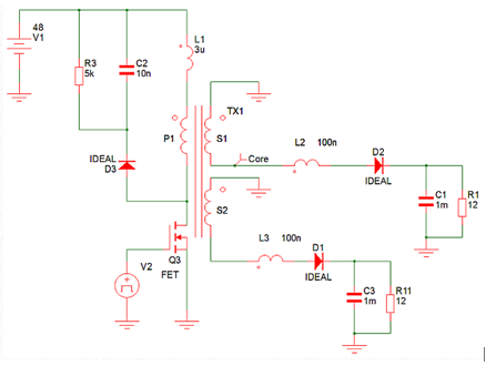
For example, a flyback power supply can generate two 12V outputs at 1A each from a 48V input, as shown in the simplified simulation model of Figure 1. The ideal diode model has zero forward voltage drop and negligible resistance. The transformer winding resistance is negligible, and only the parasitic inductances in series with the transformer leads can be modeled. These inductors are the leakage inductance within the transformer, as well as the parasitic inductances within the printed circuit board (PCB) traces and diodes. When these inductors are set, the two outputs track each other because the full coupling of the transformer forces the two outputs to be equal when the diodes conduct during the 1-D portion of the switching cycle.

Figure 1 This simplified flyback model simulates the effect of leakage inductance on output voltage regulation.
Now consider what happens when you introduce 100 nH of leakage inductance into both secondary leads of the transformer, and 3 μH of leakage in series with the primary winding. These inductances create parasitic inductances in the current path, which include leakage inductance inside the transformer and inductance in the PCB and other components. When the initial field effect transistor (FET) turns off, the initial leakage inductance still has current flowing, and the secondary leakage inductance starts a 1-D cycle with an initial condition of 0 A. A pedestal voltage appears across the transformer core, common to all windings. This pedestal voltage causes the current in the primary leakage to ramp down to 0 A, and causes the secondary leakage current to ramp up to deliver current to the load.
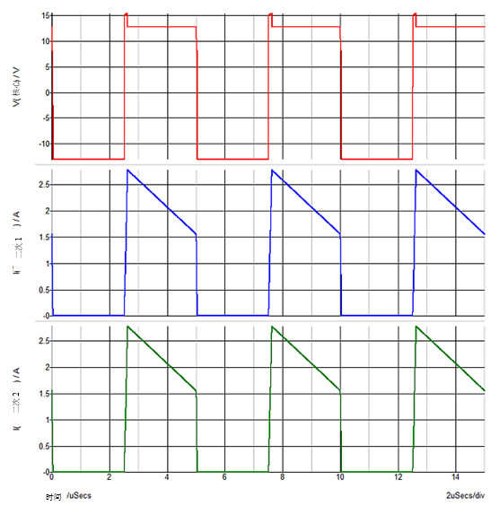
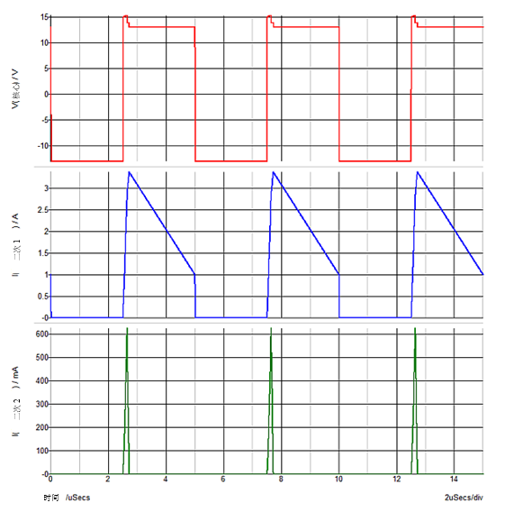
When both outputs are heavily loaded, current continues to flow throughout the 1-D cycle and the output voltages are well balanced, as shown in Figure 2. However, when one output is heavily loaded and the other lightly loaded, the output capacitor on the lightly loaded output tends to peak charge from this pedestal voltage; its output diode stops conducting because the current quickly ramps back to zero. See the waveforms in Figure 3. The cross-regulation effect of these peak charging parasitic inductors is typically much worse than that caused by the rectifier forward voltage drop alone.

Figure 2 When a heavy load is applied to both outputs, secondary current flows in both secondary windings over the entire 1-D cycle. You can see the pedestal voltage on the upper red trace.

Figure 3. Heavily loaded secondary 1 and lightly loaded secondary 2. The base voltage charges the output capacitor of secondary 2 at its peak.
Synchronous rectifiers help alleviate this problem by forcing current to flow in both windings throughout the 1-D cycle, regardless of the load. Figure 4 shows the waveform with the same load conditions as Figure 3, but with ideal synchronous rectifiers replacing the ideal diodes. Because the synchronous rectifiers hold up well after the base voltage drops, the two output voltages track each other well, even with severely unbalanced loads.
Although the average current in secondary 2 is very small, the root mean square (RMS) content can still be quite high. This is because, unlike the ideal diode in Figure 3, the synchronous rectifier forces continuous current flow during the entire 1-D cycle. Interestingly, the current must be negative for most of this cycle to ensure a low average current.
Obviously, you sacrifice better regulation for higher circulating current. However, this does not necessarily mean that the total losses will be higher. The forward voltage drop of a synchronous rectifier is usually much lower than that of a diode, so the efficiency of a synchronous rectifier at higher loads is usually much better.
![]()
![]()

Figure 4 A synchronous rectifier is used instead of a diode to force current to flow in both secondary windings and eliminate the peak charging of the base voltage.
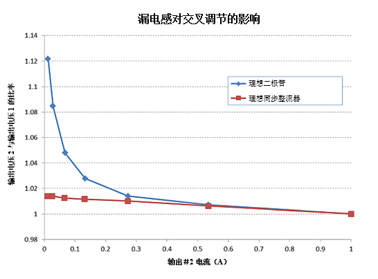
You can see the effect on cross regulation in Figure 5. The load on output 1 remains stable at 1A, while the load on output 2 fluctuates between 10 mA and 1A. At loads below 100 mA, cross regulation is severely degraded when diodes are used due to the effect of charging the base voltage peak.
Keep in mind that you are only seeing the effects of leakage inductance because ideal diodes and ideal synchronous rectifiers are used in these simulations. The benefits of using synchronous rectifiers are further highlighted when the effects of resistance and the forward voltage drop of the rectifiers are considered.
Therefore, to achieve excellent cross-regulation in a multi-output flyback power supply, consider using synchronous rectifiers. In addition, you may also improve the efficiency of the power supply. Check out TI 's 40V to 60V Input 40W Dual-Output Isolated Flyback Converter (6V at 4.33A) and Class 3 Dual-Output Isolated Flyback Converter for PoE Applications reference designs as examples of flyback power supplies using synchronous rectifiers.
![]()

Figure 5 This graph shows the cross-regulation between the two outputs, where the 1-A load on Output 1 remains stable while the load on Output 2 varies, highlighting how synchronous rectifiers mitigate the effects of leakage inductance.
Previous article:How to quickly locate and troubleshoot power module faults
Next article:How to start power supply design
- Popular Resources
- Popular amplifiers
- MathWorks and NXP Collaborate to Launch Model-Based Design Toolbox for Battery Management Systems
- STMicroelectronics' advanced galvanically isolated gate driver STGAP3S provides flexible protection for IGBTs and SiC MOSFETs
- New diaphragm-free solid-state lithium battery technology is launched: the distance between the positive and negative electrodes is less than 0.000001 meters
- [“Source” Observe the Autumn Series] Application and testing of the next generation of semiconductor gallium oxide device photodetectors
- 采用自主设计封装,绝缘电阻显著提高!ROHM开发出更高电压xEV系统的SiC肖特基势垒二极管
- Will GaN replace SiC? PI's disruptive 1700V InnoMux2 is here to demonstrate
- From Isolation to the Third and a Half Generation: Understanding Naxinwei's Gate Driver IC in One Article
- The appeal of 48 V technology: importance, benefits and key factors in system-level applications
- Important breakthrough in recycling of used lithium-ion batteries
- LED chemical incompatibility test to see which chemicals LEDs can be used with
- Application of ARM9 hardware coprocessor on WinCE embedded motherboard
- What are the key points for selecting rotor flowmeter?
- LM317 high power charger circuit
- A brief analysis of Embest's application and development of embedded medical devices
- Single-phase RC protection circuit
- stm32 PVD programmable voltage monitor
- Introduction and measurement of edge trigger and level trigger of 51 single chip microcomputer
- Improved design of Linux system software shell protection technology
- What to do if the ABB robot protection device stops
- Huawei's Strategic Department Director Gai Gang: The cumulative installed base of open source Euler operating system exceeds 10 million sets
- Download from the Internet--ARM Getting Started Notes
- Learn ARM development(22)
- Learn ARM development(21)
- Learn ARM development(20)
- Learn ARM development(19)
- Learn ARM development(14)
- Learn ARM development(15)
- Analysis of the application of several common contact parts in high-voltage connectors of new energy vehicles
- Wiring harness durability test and contact voltage drop test method
- [Automatic clock-in walking timing system based on face recognition] Maixbit K210 serial communication protocol debugging
- CAN bus receives error information? Add CRC check in the data?
- Working principle, purpose and use of flexible waveguide
- Motor Control Basics - Timer Encoder Mode Usage and Speed Calculation
- Thank you-Chengdu
- [Xianji HPM6750 Review 7] A video player that reads RGB data files from an SD card
- TMS570LS erases BANK0
- 2012 Competition Award-winning Papers, Source Code, PCB (Part 4)
- Hey guys, can you tell me what DFX design is?
- Condensing exclusive technology - Nichicon's on-board charger solution

 TL084X2DBLE


 京公网安备 11010802033920号