A long-standing challenge for designers of MP3 players, personal media players, digital cameras, and other portable consumer applications is to achieve high performance and low power consumption. These battery-powered systems typically use an embedded digital signal processor ( DSP ) that maximizes processing power when the system is processing multimedia applications and minimizes power consumption when the system is in sleep mode . Battery life is a very important metric in handheld products, and the success of the product is directly related to the efficiency of the power supply system.
A key component in such systems is a step-down DC-DC switching regulator that can efficiently derive a lower supply voltage from a higher voltage, such as 1V from 4.5V. As a regulator , it must maintain a constant voltage and respond quickly to changes in input voltage and load current. The architecture discussed in this article has excellent voltage regulation performance as well as the advantages of high efficiency and fast response.
Anatomy of a Switching Regulator
Figure 1 shows a typical application circuit for the Analog Devices ADP2102, a low duty cycle, 3 MHz synchronous rectifier step-down converter. The ADP2102 has multiple configurations for fixed and adjustable output voltages. Here the ADP2102 is connected in a fixed output voltage configuration to generate a 300mA, 0.8 V output voltage from a 5.5 V input voltage. Next is an application example with adjustable output voltage.
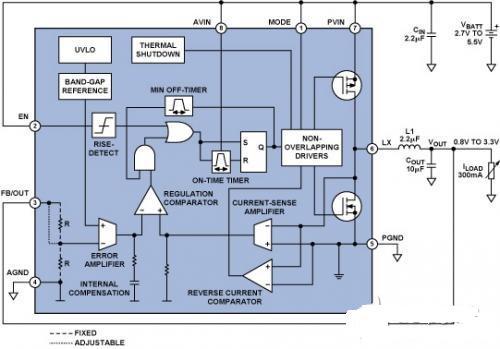
Figure 1. Generating a 0.8 V output from a 5.5 V input using the ADP2102.
Here is a brief explanation of the working principle of the circuit: the divided voltage of the DC output voltage is compared with the internal reference source in the error amplifier, and then the output of the error amplifier is compared with the output of the current sampling amplifier to drive the monostable trigger. The monostable trigger is in a quasi-stable state for a time period determined by VOUT/VIN. The monostable trigger turns on the upper gate transistor, and the current in the inductor L1 gradually increases. When the quasi-stable state of the monostable trigger ends, the transistor is turned off, and the current in the inductor L1 gradually decreases. After a time interval determined by the minimum off-time timer and the minimum ("valley") current, the monostable trigger is triggered again. The monostable trigger timer inside the chip uses input voltage feedforward to maintain a constant frequency in steady state.
This oscillation continues at an indeterminate frequency (approximately 3 MHz), but can be deviated from this frequency if necessary in response to line and load transients so that the output voltage remains constant and the average value of the inductor current is maintained at the current required by the output load.
The method described above is relatively new. For many years, the dominant method for DC-DC conversion has been the constant frequency peak current method, also known as trailing edge modulation when implemented in a step-down DC-DC converter. A detailed description of this method, an evaluation of its advantages and disadvantages, and the constant on-time valley current mode converter described above can be found in other technical articles.
The ADP2012 also features undervoltage lockout, soft-start, overtemperature protection, and short-circuit protection, and has ±1% feedback accuracy. This architecture enables the main switch on-time to be as low as 60 ns or less.
Figure 2 shows typical waveforms under different conditions. Figure 2a shows the low duty cycle when ILOAD = 600mA and the voltage decreases from VIN = 5.5V to VOUT = 0.8V. As shown in the figure, at a switching frequency of 3MHz, a minimum on-time of 45ns can be obtained.
FIG2b shows the load current and inductor current waveforms when the load current suddenly increases by 300mA.
FIG2c shows the load current and inductor current waveforms when the load current suddenly decreases by 300 mA.
Figure 2d shows that there is no subharmonic oscillation at a duty cycle of 50%, which must be considered in the design when using peak current mode control. There is also no subharmonic oscillation when the duty cycle is greater or less than 50%.
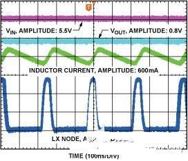
Figure 2a. VIN = 5.5 V, VOUT = 0.8 V, minimum on-time = 45 ns
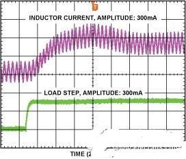
Figure 2b. Sudden load transient response (ILOAD = 300 mA)
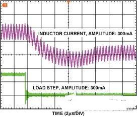
Figure 2c. Sudden load drop transient response (ILOAD = 300 mA)
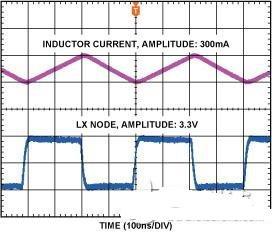
Figure 2d. Duty cycle = 50%, VIN = 3.3 V, VOUT = 1.8 V, ILOAD = 300 mA
Dynamic Voltage Scaling in DSP Applications
In portable applications using DSPs, the core voltage and I/O voltage of the DSP are usually provided by switching converters, which requires the use of high-efficiency DC-DC converters for battery-powered applications. The regulator that provides the core voltage must be able to dynamically change the voltage based on the processor's clock speed or dynamically change the voltage according to software instructions. In addition, the small size of the overall solution is equally important.
Here, we describe how to replace the internal regulator of the Blackfin processor with an external high-efficiency regulator to improve system power efficiency in battery-powered applications. Furthermore, we describe the control software for the external regulator.
Dynamic Power Management
The power consumption of a processor is proportional to the square of the operating voltage (VCORE) and proportional to the operating frequency (FSW). Therefore, reducing the frequency can reduce dynamic power consumption linearly, while reducing the core voltage can reduce dynamic power consumption exponentially.
In power-sensitive applications, when the DSP is simply monitoring system activity or waiting for an external trigger, changing the clock frequency while maintaining the supply voltage is very useful for reducing power consumption. However, in high-performance battery-powered applications, changing the frequency alone does not significantly save power. Blackfin processors and other DSPs with advanced power management features can change the core voltage and frequency in turn, thereby achieving optimal battery utilization in all situations.
Dynamic voltage regulation in the ADSP -BF53x series Blackfin processors is usually achieved by an internal voltage controller and an external MOSFET. The advantage of this method is that a single voltage (VDDEXT) can be applied to the DSP subsystem, and the required core voltage (VDDINT) can be obtained from the MOSFET. The core voltage can be software controlled through internal registers to control MIPS and ultimately control energy consumption, thereby achieving optimal battery life.
In order to fully implement the Blackfin internal voltage regulation solution, an external MOSFET, Schottky diode, large inductor and multiple output capacitors are required. This solution is relatively expensive, but the efficiency is very poor, and the PCB board area occupied is relatively large, which brings a great contradiction to system designers. The need to use large inductors and capacitors in the integrated voltage regulator is not conducive to the miniaturization of portable devices as much as possible as consumers want. The efficiency of the integrated voltage regulator controller is relatively low, usually only 50%~70%, so this method is not suitable for high-performance handheld battery-powered applications.
External voltage regulation
New DC-DC switching converter design methods can improve the efficiency of the Blackfin integration approach itself to 90% or more. In addition, the size of external components can be reduced when using external regulators .
A variety of dynamic voltage scaling (DVS) control schemes can also be used, including switched resistors (which can be implemented by a DAC in some cases) and pulse width modulation (PWM) (which can achieve the same accuracy as the internal method). Regardless of which scheme is used, it must be possible to change the regulation level through software control. The above regulation control methods are integrated in the internal regulator , but must be implemented through external devices in external regulation.
This article describes two methods of regulating the DSP core voltage using the ADP2102 synchronous dc-to-dc converter, dynamically adjusting the core voltage from 1.2 V to 1.0 V when the processor is running at low clock speeds.
The ADP2102 high-speed synchronous switching converter can reduce the core voltage to 0.8 V when powered by a battery voltage of 2.7V~5.5V. Its constant on-time current mode control and 3MHz switching frequency provide excellent dynamic response, very high efficiency and excellent source regulation and load regulation. The higher switching frequency allows the system to use ultra-small multilayer inductors and ceramic capacitors. The ADP2102 uses a 3 mm×3 mm LFCSP package, which saves space and requires only three or four external components. In addition, the ADP2102 includes complete functions, such as various safety features, such as undervoltage lockout, short-circuit protection, and overheating protection.
Figure 3 shows the circuit to implement DVS. The 3.3 V supply on the ADSP-BF533 EZ-KIT Lite evaluation board powers the step-down converter ADP2102, and the output voltage of the ADP2102 is set to 1.2 V using the external resistor divider R1 and R2. The GPIO pin of the DSP is used to select the desired core voltage. Changing the feedback resistor value can adjust the core voltage in the range of 1.2 V to 1.0 V. The N-channel MOSFET can modify the voltage divider by resistor R3 in parallel with R2. Compared to R3, the RDSon of the IRLML2402 is small, only 0.25Ω. The 3.3 V GPIO voltage is used to drive the gate of the MOSFET. In order to obtain better transient performance and improve load regulation, a feed-forward capacitor CFF needs to be added.
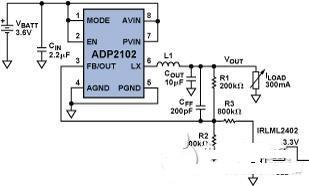
Figure 3. Dynamic voltage scaling of the ADP2102 using external MOSFETs and Blackfin PWM control.
For dual-level switches, general application requirements are:
DSP core voltage (VOUT1) = 1.2 V
DSP core voltage (VOUT2) = 1.0 V
Input voltage = 3.3 V
Output current = 300 mA
Using high-value divider resistors can minimize power losses. Feedforward capacitors reduce the effect of gate-drain capacitance during switching. Overshoot or undershoot caused by this transient can be minimized by using smaller feedback resistors and larger feedforward capacitors, but this comes at the expense of additional power dissipation.
Figure 4 shows the output current IOUT, the output voltage VOUT, and the control voltage VSEL. When VSEL is low, the output voltage is 1.0 V, and when VSEL is high, the output voltage is 1.2 V.
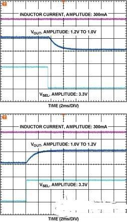
Figure 4. Adjusting the feedback resistor below the MOSFET
A simpler method to generate two different voltages for DVS uses a control voltage VC to inject current into the feedback network through an additional resistor. Adjusting the duty cycle of the control voltage changes its average DC level. Thus, the output voltage can be adjusted using a control voltage and resistor. The following formulas are used to calculate the values of resistors R2, R3 and the control voltage amplitude levels VC_LOW and VC_HIGH.
(1)
(2)
For VOUT1 = 1.2 V, VOUT2 = 1.0 V, VFB = 0.8 V, VC_LOW = 3.3 V, VC_HIGH = 0 V, and R1 = 49.9 kohm, R2 and R3 can be calculated as follows
(3)
(4)
This method produces a smoother transition. Unlike the MOSFET switching method, any control voltage that can drive a resistive load can be used for this scheme, while the MOSFET switching method can only be used for control signal sources that drive capacitive loads. This method can be applied to any output voltage combination and output load current. Therefore, by adjusting the core voltage as needed, the power consumption of the DSP can be reduced . Figure 5 shows the transition between two output voltages using this current injection method.
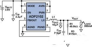
Figure 5. Dynamic voltage adjustment of the ADP2102 using control voltage VC.
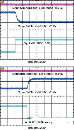
Figure 6. Adjusting the feedback resistor below by controlling the voltage
Previous article:Design of power distribution control module based on LPC2119
Next article:Analysis of Startup Performance of UCC2870 Primary Control Flyback Power Supply Controller
Recommended ReadingLatest update time:2024-11-23 11:22

- Popular Resources
- Popular amplifiers
- RAQ #223: How to measure and determine soft-start timing without a soft-start equation?
- Vicor high-performance power modules enable the development of low-altitude avionics and EVTOL
- Bourns Launches Two Thick Film Resistor Series with High Power Dissipation Capabilities in Compact TO-220 and DPAK Package Designs
- Bourns Launches New High-Pulse Brake Resistor Series with Superior Energy Dissipation Capabilities
- Nexperia launches new 120 V/4 A half-bridge gate driver to further improve robustness and efficiency in industrial and automotive applications
- Vishay's New 150 V MOSFETs Offer Industry-Leading Power Loss Performance
- The first generation of SGT MOSFET series from Qiangmao: innovative trench technology, automotive-grade 60 VN channel, breakthrough in high-efficiency performance of automotive electronics
- DC/DC Power Supplies for Automotive Applications
- MathWorks and NXP Collaborate to Launch Model-Based Design Toolbox for Battery Management Systems
- Intel promotes AI with multi-dimensional efforts in technology, application, and ecology
- ChinaJoy Qualcomm Snapdragon Theme Pavilion takes you to experience the new changes in digital entertainment in the 5G era
- Infineon's latest generation IGBT technology platform enables precise control of speed and position
- Two test methods for LED lighting life
- Don't Let Lightning Induced Surges Scare You
- Application of brushless motor controller ML4425/4426
- Easy identification of LED power supply quality
- World's first integrated photovoltaic solar system completed in Israel
- Sliding window mean filter for avr microcontroller AD conversion
- What does call mean in the detailed explanation of ABB robot programming instructions?
- STMicroelectronics discloses its 2027-2028 financial model and path to achieve its 2030 goals
- 2024 China Automotive Charging and Battery Swapping Ecosystem Conference held in Taiyuan
- State-owned enterprises team up to invest in solid-state battery giant
- The evolution of electronic and electrical architecture is accelerating
- The first! National Automotive Chip Quality Inspection Center established
- BYD releases self-developed automotive chip using 4nm process, with a running score of up to 1.15 million
- GEODNET launches GEO-PULSE, a car GPS navigation device
- Should Chinese car companies develop their own high-computing chips?
- Infineon and Siemens combine embedded automotive software platform with microcontrollers to provide the necessary functions for next-generation SDVs
- Continental launches invisible biometric sensor display to monitor passengers' vital signs
- [Internal training materials] Essential knowledge points on BMS and PEPS related devices, DSRC Internet of Vehicles, and T-BOX Internet of Vehicles
- F350 pwm configuration failed
- [MM32 eMiniBoard Review] ADC collects potentiometer data and sends it to the computer for display via USB-CDC
- Has anyone made a circuit that triggers a low level for 2ms and then maintains the low level for 80ms?
- Device selection - What parameters should be paid attention to when selecting TVS tubes?
- I won an Apple computer at the annual meeting, but the company I left wants to take it back. What should I do?
- Application of Polymer Capacitors in DC-DC Converters
- Everyone is paying attention to Qorvo's broadband access CATV and FTTH products
- How to make a web configuration with ESP8266
- When using STM32F407 to send data manually, the data is sometimes not sent completely and some contents cannot be displayed in the serial assistant.

 Battery Management Systems for Electric and Hybrid Vehicles


 京公网安备 11010802033920号