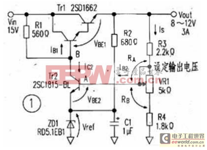
Figure 1 is a voltage- regulated power supply with adjustable output voltage using a transistor . This circuit adjusts the output voltage by changing the voltage drop of the high-power transistor Tr1 connected in series with the load. The output voltage Vout is determined by the voltage at point A, i.e., Vref+VBE2.

Where Vref is the voltage of the Zener diode (5.1V), VBE2 is the voltage between the base and emitter of transistor Tr2 (0.65V>, and VR1 is a variable resistor. Since the resistance value of VR1 varies from 0 to 5kΩ, the output voltage varies from 7.6 to 12.8V. When the sliding part of VR1 has poor contact, the output voltage will become the minimum voltage.
The maximum power consumption of the adjustment tube Tr1 is 3A×(15V-8V)=21W, so it should be installed on a heat sink below 4℃/W. Since VBE2 will change with temperature and IC2, the voltage regulation circuit and voltage regulation characteristics are not very good.


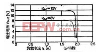
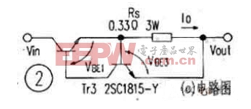
In the circuit of Figure 1, the circuit does not have an overcurrent protection function. When a short circuit occurs at the output end, the input 15V voltage will be fully applied to Tr1, causing Tr1 to burn out instantly. Figure 2(a) is an overcurrent protection circuit. By adding a series resistor Rs and a small power transistor Tr3 to the emitter circuit of Tr1, the current flowing through Tr1 can be limited when a short circuit occurs at the output end of the circuit. In normal operation, Tr3 is cut off because the voltage drop on the Rs resistor is very small. When the output current of the circuit increases, the voltage drop on the RS resistor also increases. When the voltage drop on the RS resistor (VBE3 of Tr3) exceeds 0.65V, Tr3 is turned on and the VCE of Tr3 decreases. The VBE1 of Tr1 also decreases, so the output current flowing through Tr1 will be limited to a certain set value. In this circuit, the current limit value is 0.65V/Rs≈2A. In addition, the circuit of Figure 2(a) can also be used as a constant current source circuit for light-emitting diodes. When applied, the output end of the circuit in Figure 2(a) is grounded, and the collector of Tr1 is connected to the light-emitting diode. Figure 2(b) shows the current limiting characteristics of the circuit.
Previous article:A design scheme of linear precision voltage regulated power supply based on TL431
Next article:Teach you a simple DIY design of a voltage-stabilized power supply
- Popular Resources
- Popular amplifiers
- MathWorks and NXP Collaborate to Launch Model-Based Design Toolbox for Battery Management Systems
- STMicroelectronics' advanced galvanically isolated gate driver STGAP3S provides flexible protection for IGBTs and SiC MOSFETs
- New diaphragm-free solid-state lithium battery technology is launched: the distance between the positive and negative electrodes is less than 0.000001 meters
- [“Source” Observe the Autumn Series] Application and testing of the next generation of semiconductor gallium oxide device photodetectors
- 采用自主设计封装,绝缘电阻显著提高!ROHM开发出更高电压xEV系统的SiC肖特基势垒二极管
- Will GaN replace SiC? PI's disruptive 1700V InnoMux2 is here to demonstrate
- From Isolation to the Third and a Half Generation: Understanding Naxinwei's Gate Driver IC in One Article
- The appeal of 48 V technology: importance, benefits and key factors in system-level applications
- Important breakthrough in recycling of used lithium-ion batteries
- LED chemical incompatibility test to see which chemicals LEDs can be used with
- Application of ARM9 hardware coprocessor on WinCE embedded motherboard
- What are the key points for selecting rotor flowmeter?
- LM317 high power charger circuit
- A brief analysis of Embest's application and development of embedded medical devices
- Single-phase RC protection circuit
- stm32 PVD programmable voltage monitor
- Introduction and measurement of edge trigger and level trigger of 51 single chip microcomputer
- Improved design of Linux system software shell protection technology
- What to do if the ABB robot protection device stops
- How haptic technology can enhance driving safety
- Let’s talk about the “Three Musketeers” of radar in autonomous driving
- Why software-defined vehicles transform cars from tools into living spaces
- How Lucid is overtaking Tesla with smaller motors
- Wi-Fi 8 specification is on the way: 2.4/5/6GHz triple-band operation
- Wi-Fi 8 specification is on the way: 2.4/5/6GHz triple-band operation
- Vietnam's chip packaging and testing business is growing, and supply-side fragmentation is splitting the market
- Vietnam's chip packaging and testing business is growing, and supply-side fragmentation is splitting the market
- Three steps to govern hybrid multicloud environments
- Three steps to govern hybrid multicloud environments
- This problem occurs when setting up the stm8 environment. What is the reason? Thank you
- dsp28335 data space
- [Xianji HPM6750 Review 8] Detailed description of the small twists and turns encountered by SPI peripherals
- MSP430 MCU Development Record (16)
- I posted a thread about icebabycool. He didn't answer the question but laughed at me instead of showing my low IQ. Please punish this kind of rogue behavior severely.
- Help with POE design issues
- [Voice and vision module based on ESP32S3] Material unpacking—ESP32S3 BOX
- PCBA intelligent detection fixture, one-click generation of test reports
- How to choose the right inductor in a switching power supply
- EEWORLD University Hall----Introduction to Isolated Modulator

 5962-9553601QHA


 京公网安备 11010802033920号