Countries are increasingly stringent in their requirements for the power factor of LED bulbs , making the design of LED driver circuits increasingly challenging. Therefore, semiconductor companies have developed a new generation of LED driver solutions that can take into account the requirements of small size, high energy efficiency and high power factor by improving the buck topology, helping developers to design LED bulbs with a power factor of more than 0.9.
随着白炽灯泡逐步被淘汰,节能萤光灯(CFL)和发光二极体(LED)将成为提供显著节能效果的两种照明选择。尽管CFL技术成熟,然白光LED发展快速,每颗LED元件的输出流明与光效已愈来愈高。LED灯泡的使用寿命是标准白炽灯泡二十五倍以上,且光效已超越CFL灯泡的性能水平。
The electronic ballast in most common CFL bulbs is a capacitor type, with a typical power factor (PF) of 0.5 to 0.6. This means that although the household only pays for the power indicated on the bulb, the power company actually has to generate a proportional amount of volt-amps, so a 13-watt CFL bulb with a power factor of 0.5 represents a load of 26 volt-amps, which is only slightly less than 50% of the volt-amps of a 60-watt incandescent bulb.
Therefore, the US Energy Star stipulates that the minimum power factor of LED bulbs with a power greater than 5 watts must be 0.7, and the minimum power factor of commercial LED lamps such as recessed lights and spotlights must reach 0.9. Looking around the world, the US does not have the most stringent requirements on the power factor of LED bulbs ; the most stringent is South Korea, which requires that all lights with an input power greater than 5 watts must have a minimum power factor of 0.9. This requirement will bring challenges to designers of LED drive circuits, who must comprehensively evaluate energy efficiency, available space and overall bill of materials (BOM) costs to provide optimized LED lighting solutions.
The introduction of buck topology circuit has made a great leap forward in the PF of LED bulbs
Incandescent bulbs are designed for a specific line voltage, but designers do not need to consider how to make a universally designed LED bulb popular around the world. In addition, the power supply in the LED bulb does not need to be electrically isolated from the load because it is integrated into a single housing; but attention must still be paid to the design of the mechanism, which must meet safety requirements in a physical way. With this in mind, designers no longer need to rely on isolated flyback topology as the only power conversion architecture option.
Under certain boundary conditions, the buck topology can be optimized to provide good power factor. To provide high power factor, the input current must be consistent with the line and increase proportionally with the increase of the rectified line voltage. The disadvantage of the buck topology is that the current will not flow until the input voltage Vin is greater than the output voltage Vout, so the LED string voltage must be low compared to the line voltage. In most cases, this is not a problem because the number of LEDs in series is relatively small compared to the line voltage. For example, the total voltage of eight LEDs in series is about 25 volts, which is less than 15% of the peak voltage of the rectified 120 volt AC input.
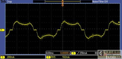
One control method for high power factor boost converters is fixed on-time control, where the switching cycle restarts when the inductor current reaches zero. To control power, designers must use feedback to adjust the on-time, and the same concept can be applied to buck topologies . With a fixed on-time, the current through the inductor/switch rises in direct proportion to the line, providing a near-perfect power factor, with the tradeoff being that the peak current at the top of the switching cycle can be very large. Light bulb applications do not require an excellent power factor; therefore, if the peak current is limited during a portion of the switching cycle, the losses in the switch and inductor can be reduced, providing higher conversion efficiency and limiting the size of the inductor. The typical line current waveform produced by this method is not as close to a sinusoidal curve as shown in Figure 1. However, the waveform produced by this method easily provides a power factor greater than 0.9, but the tradeoff is increased distortion.
Figure 1 Input current waveform improves the PF of the bulb. LED controller plays a key role
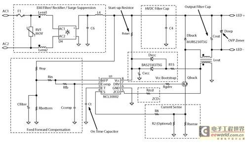
To apply this fixed on-time/peak current hybrid mechanism, semiconductor manufacturers developed the NCL30002 controller (Figure 2).
Figure 2 Power factor correction buck application circuit diagram
From the controller circuit diagram, it can be observed that the LED is referenced to the high voltage rail; while the power switch is referenced to the ground, which is called reverse buck. It can simplify the architecture mainly because it can directly sense the peak LED current and drive the unijunction field effect transistor (FET) without the use of a level shifter.
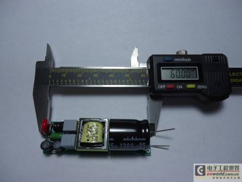
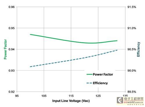
After the controller starts the switch, the driver is biased from the auxiliary winding on the inductor, thus adding a function that can sense the inductance and when the current drops to zero, it indicates that a new switching cycle should begin. A precise 485 millivolt (mV) voltage (typical accuracy ±2%) is used to regulate the peak current flowing through the switch. When Vin exceeds LEDVf, the fixed on-time control is used to adjust the power to the LED until the peak current limit is reached, which can be detected by the sense resistor Rsense. In order to control the power provided by the AC line voltage under the rated voltage variation, the line feedforward compensation is used to modulate the on-time. Here is an example of an 18-watt LED driver circuit that is suitable for being incorporated into an LED bulb that replaces a 75-watt A-type bulb, driving a string of eight LEDs at 750 milliamperes , with an output ripple of less than ±30%. Figure 3 is a photo of the 18 mm x 60 mm circuit board of this design example; Figure 4 shows that the typical energy efficiency is greater than 90% and the power factor is greater than 0.94.
Figure 4 Typical performance at 18.5W (24.7V @ 750mA) output
如上所述,采用优化架构可以解决兼顾小体积、高能效且符合一体式LED灯泡最严格功率因数要求的设计难题。设计人员透过改变金属氧化物半导体场效电晶体(MOSFET)及减小电感尺寸,可以调校LED灯泡基本设计,用于更低功率的应用。此点至关重要的原因在于,LED制造商增加每颗LED的流明输出,使LED光效持续提升,进而要求能以更少的LED提供相同流明输出,藉此降低功耗,并减少一体式灯泡的成本,增加市场接受度。
Previous article:LED power supply solution based on Mean Well switching power supply
Next article:Engineer technology sharing: an effective LED switch power supply protection design
- Popular Resources
- Popular amplifiers
- MathWorks and NXP Collaborate to Launch Model-Based Design Toolbox for Battery Management Systems
- STMicroelectronics' advanced galvanically isolated gate driver STGAP3S provides flexible protection for IGBTs and SiC MOSFETs
- New diaphragm-free solid-state lithium battery technology is launched: the distance between the positive and negative electrodes is less than 0.000001 meters
- [“Source” Observe the Autumn Series] Application and testing of the next generation of semiconductor gallium oxide device photodetectors
- 采用自主设计封装,绝缘电阻显著提高!ROHM开发出更高电压xEV系统的SiC肖特基势垒二极管
- Will GaN replace SiC? PI's disruptive 1700V InnoMux2 is here to demonstrate
- From Isolation to the Third and a Half Generation: Understanding Naxinwei's Gate Driver IC in One Article
- The appeal of 48 V technology: importance, benefits and key factors in system-level applications
- Important breakthrough in recycling of used lithium-ion batteries
- LED chemical incompatibility test to see which chemicals LEDs can be used with
- Application of ARM9 hardware coprocessor on WinCE embedded motherboard
- What are the key points for selecting rotor flowmeter?
- LM317 high power charger circuit
- A brief analysis of Embest's application and development of embedded medical devices
- Single-phase RC protection circuit
- stm32 PVD programmable voltage monitor
- Introduction and measurement of edge trigger and level trigger of 51 single chip microcomputer
- Improved design of Linux system software shell protection technology
- What to do if the ABB robot protection device stops
- Keysight Technologies Helps Samsung Electronics Successfully Validate FiRa® 2.0 Safe Distance Measurement Test Case
- Innovation is not limited to Meizhi, Welling will appear at the 2024 China Home Appliance Technology Conference
- Innovation is not limited to Meizhi, Welling will appear at the 2024 China Home Appliance Technology Conference
- Huawei's Strategic Department Director Gai Gang: The cumulative installed base of open source Euler operating system exceeds 10 million sets
- Download from the Internet--ARM Getting Started Notes
- Learn ARM development(22)
- Learn ARM development(21)
- Learn ARM development(20)
- Learn ARM development(19)
- Learn ARM development(14)
- MSP430 driver function for LCD1602
- With vias in vogue, where will high-speed DDR4 signals go?
- Micropython can be simulated in proteus
- EEWORLD University Hall----Live Replay: Introduction of ON Semiconductor's Photovoltaic and Energy Storage Products
- Watch the video to win a JD card | Taixiang test of Shuige cheats
- The motor coil is an inductive load, so the current in the coil will have a certain delay relative to the load voltage on the coil.
- Summary of national competition experience sharing
- How to understand the equivalent of capacitors passing AC
- [NXP Rapid IoT Review] +6. Guide to Translation Display Elements
- MicroPython driver porting for STTS751


 QPB7425SR


 京公网安备 11010802033920号