The luminous efficiency of light-emitting diodes ( LEDs ) is much higher than that of traditional light sources, and the power consumption is only about 20% of that of traditional light sources of the same brightness. They are also environmentally friendly and healthy, with small size, long life, high efficiency, and mercury-free. In addition, the efficiency of current LED products has exceeded 110 lumens per watt, and the application field of LEDs is infinitely broad. In particular, driven by emerging markets such as lighting , notebook computers/LCD TV backlight modules, the global LED market size grew significantly in 2010, reaching US$9.6 billion. In addition, with the promotion of energy-saving policies in various countries around the world, the penetration rate of LED lighting in the lighting market has exceeded 3%, and the overall output value has reached US$4 billion. It is estimated that by 2015, the global LED lighting market penetration rate will reach 20%; starting in 2020, the popularization of LED lighting will be gradually realized and become the main application of the LED industry.
Since the 311 nuclear disaster, Japanese consumers have purchased a large number of LED bulbs to save energy, indicating that the era of LED lighting has arrived. In order to achieve the goal of energy saving in lighting, governments of various countries have also issued relevant policies in recent years, such as the US "Energy Star" program, Japan's "Eco-Point" system, South Korea's "15/30" and "Green LED Lighting Popularization Development Program", China's "Eleventh Five-Year Plan" and "Twelfth Five-Year Plan" and other green energy policies. Major countries such as the United States and Japan have also drawn up technology research and development blueprints and are committed to developing high-efficiency solid-state lighting technology to improve energy efficiency and significantly reduce greenhouse gas emissions, so as to reduce greenhouse gas emissions in developed countries by 25~40% by 2020 compared to 1990.
However, currently commercialized GaN semiconductor optoelectronic components are mainly based on sapphire and silicon carbide (SiC) substrates. In order to replace existing lighting products, efficiency and cost are the goals that all manufacturers strive for. Therefore, in recent years, GaN on Si has gradually challenged the position of GaN on Sapphire with its large size and low cost advantages; on the other hand, GaN on GaN has gradually emerged with its high performance and high current operation advantages. At present, Sorra in the United States has launched products based on c-plane GaN substrates. In the future, combining the overall advantages of GaN on GaN with the reduction of substrate costs, it is expected that in 2015, it will have the opportunity to replace LED lighting solutions.
Thanks to technological breakthroughs, GaN now has many crystal orientations that can be used as LED substrates , including the traditional polar c-plane, non-polar m-plane and a-plane, and semi-polar (11-22), (10-12), (20-2-1) and (20-21) planes. Regardless of which surface, many research teams have published papers on the performance of LEDs. However, considering the overall mature technology, substrate size and cost, the c-plane GaN substrate is still the most competitive. Therefore, the advantages of GaN on c-plane GaN LED are summarized as follows: high-quality epitaxial film, lattice constant matching between epitaxial film and substrate, vertical device structure and short epitaxial time. The defect density of the GaN substrate used in the following experiment is 105~106cm-2.
GaN on GaN efficiency is stable without being affected by lattice constant mismatch
At present, the light-emitting layer of the GaN series is mainly composed of GaN and InGaN materials. Due to the lack of substrates that match the substrate lattice, this type of light-emitting diode is generally epitaxially grown on a sapphire substrate.
However, due to the mismatch in lattice constants between the heteroepitaxially grown film and the substrate, an extremely high defect density (about 109~1010cm-2) is generated in the nitride film, which further leads to a decrease in the LED luminous efficiency. Figures 1(a)~(c) are AFM measurements of the blue light LED light-emitting layer grown on a sapphire substrate and a gallium nitride substrate. The quantum well thicknesses are 2.7 nm, 6 nm, and 15 nm, respectively. It can be found that there are many defects in the light-emitting layer grown on the sapphire substrate. As the thickness of the light-emitting layer gradually increases, the size of the hole gradually increases.
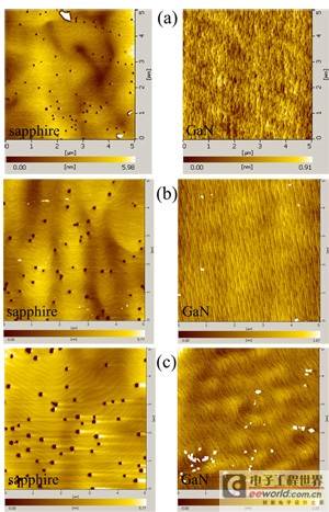
Figure 1 AFM images of blue light emitting diodes with different quantum well thicknesses (a) 2.7nm, (b) 6.0nm, and (c) 15.0nm grown on sapphire and GaN substrates
On the other hand, on the GaN substrate, there are no defects on the surface even though the thickness reaches 15 nanometers. Figure 2 is a TEM cross-sectional measurement of the GaN on GaN light-emitting layer. When the quantum well thickness is 15 nanometers, the interface between the quantum well and the quantum barrier is still very flat, and the light-emitting layer has a very good quality. From the XRD analysis of the diffraction peak wave to the half-wave width, the roughness of the quantum well interface can be estimated. On GaN on GaN, it is only about 8%, while on GaN on Sapphire it is 46.0% (Figure 3).

Figure 2 TEM cross-section of the light-emitting layer of a blue light-emitting diode grown on a GaN substrate
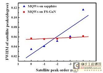
Figure 3 XRD analysis of MQW on sapphire and GaN substrate at (0002) surface
Next, a 15 mil × 15 mil conventional mesa-type device was fabricated. Under a current measurement of 200 mA (Figure 4), when the quantum well thickness of GaN on Sapphire exceeded 6 nanometers, the LED efficiency dropped very quickly, while the GaN on GaN LED only dropped slightly. This means that a thick quantum well structure can be used to increase the unit carrier density in the quantum well, which helps to reduce the Auger effect and improve the LED efficiency under high current. Furthermore, this phenomenon can also be found in experiments with different light-emitting layer logarithms and different quantum well thicknesses (Figure 5). For example, the total quantum well thickness of GaN on Sapphire has an upper limit. When this value is exceeded, the LED efficiency will drop, while the GaN on GaN efficiency can still maintain a certain value of efficiency.

Figure 4 LED efficiency diagram with different quantum well thickness on sapphire and GaN substrates
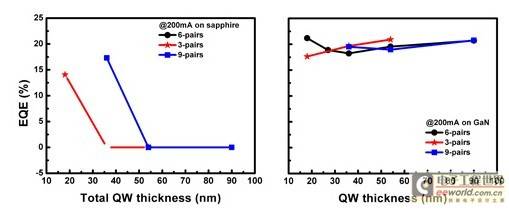
Figure 5 LED performance with different quantum well numbers and thicknesses on sapphire and GaN substrates
Homogeneous production materials GaN on GaN to avoid polarization field effects
In addition to the defects caused by lattice mismatch, traditional GaN on Sapphire also has polarization field effects caused by lattice mismatch. In contrast, GaN on GaN is a homogeneous growth material, which can reduce the polarization field effect caused by lattice constant mismatch and improve the problem of quantum efficiency reduction. Figure 6 shows that the E2(High) values of grown GaN on Sapphire and GaN on GaN are 569.52 nm and 567.16 nm, respectively. The larger value on GaN on Sapphire is caused by residual compressive stress; the value on GaN on GaN is the same as that on a pure GaN substrate, indicating that there is no stress in the GaN epitaxial film.

Figure 6 Raman analysis
Figure 7 is a graph showing the wavelength versus different current injections. When the injection current increases, a shielding effect (S CREE n Effect) will occur. Under a measurement current of 1~50mA, the LED on Sapphire has a blue shift of about 3nm; the LED on GaN has a blue shift of about 0.8nm. The smaller blue shift means that the LED on GaN has a smaller QCSE (Quantum-confined Stark Effect). From the simulation results in Figure 8, it can be seen that a smaller QCSE effect can effectively reduce the occurrence of electron overflow.
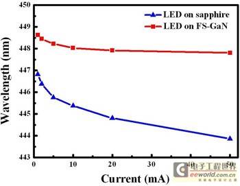
Figure 7 EL wavelength shift measurement at different currents
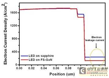
Figure 8. Electron current density simulation curve
Figure 9 is a graph of relative external quantum efficiency for current injection. Under continuous current injection, the peak value of LED on GaN appears at 20-40mA, and then begins to decline as the current rises; the peak value of LED on Sapphire is less than 20mA, and declines rapidly as the current rises. At 300mA, the external quantum efficiency of LED on Sapphire and LED on GaN is 56% and 73% for the peak value. The larger peak value of LED on GaN is caused by better material quality; at 300mA, the 38% improvement of LED on GaN is caused by improved material quality and smaller polarization field effect.

Figure 9 Relative external quantum efficiency measurements of LED on sapphire and LED on GaN under continuous current and pulse current
In pulse measurement mode, the characteristics of LED on GaN are not much different. Removing the thermal effect can improve the performance at 300mA current by 76%; while the LED on Sapphire only improves by 12%, which means that LED on Sapphire has a more serious thermal effect. When using pulse measurement, the influence of the thermal effect is ignored, thereby improving the efficiency of LED on Sapphire. This also means that in addition to the advantages of high quality and homogeneous growth, the GaN substrate itself has the advantage of high heat dissipation coefficient and can operate under large currents.
Can be used as N-type conductive substrate GaN on GaN is conducive to the production of vertical structures
The great advantage of GaN on GaN is that its substrate itself can be an N-type conductive substrate, which is conducive to the production of vertical structures. The laser lift-off process used in the traditional production of vertical structures on sapphire substrates is omitted, which can avoid the shortcomings of cumbersome processes, expensive equipment and low yields. Furthermore, the back of the gallium nitride substrate is an N-face surface, and a wet etching process can be used to simply produce a pyramid structure to improve the light extraction rate. This process is very important for improving the efficiency of gallium nitride substrates.
Due to the background doping concentration of the substrate itself, the transmittance in the visible light part cannot reach 100%. In addition, due to the difference in refractive index between the gallium nitride material and the air, most of the light is reflected back to the material itself and cannot be effectively extracted. Therefore, making a geometric pattern on the N-face surface of the gallium nitride substrate will help improve the luminous efficiency of the LED.
Figure 10 shows the etching of the GaN N-face surface at different etching times. The longer the etching time, the larger the cone size and the lower the density. Figure 11 shows the room temperature EL measurement diagram and the voltage and efficiency curve. ST-LED and RB-LED are samples without and with the wet etching process. LEDI and LEDII have emission wavelengths of 405nm and 450nm. When the wet etching process is used on the GaN substrate, the light extraction rate can be improved and the LED efficiency can be further improved. This effect is particularly significant at short wavelengths. At a current of 20mA, the overall improvement in near-ultraviolet light and blue light is 94% and 21%.
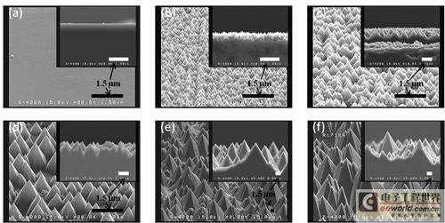
Figure 10 SEM images of the N-face surface of the GaN substrate after (a) unetched, etched, (b) 1 min, (c) 5 min, (d) 10 min, (e) 30 min, and (f) 60 min.
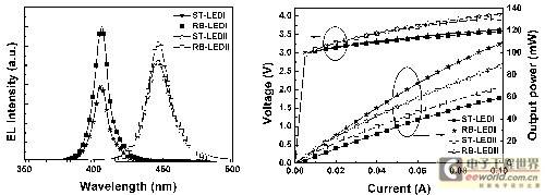
Figure 11 (a) Room temperature EL measurement and (b) LED photoelectric characteristics measurement
n-pad metal is made on the substrate GaN on GaN to shorten the epitaxy time
In addition to the high efficiency of GaN on GaN mentioned above, another major advantage is the shortened epitaxy time. Traditionally, epitaxy growth of LED on Sapphire often requires substrate baking time, low-temperature buffer layer and GaN epitaxial film growth time with a thickness of more than 4 microns. The overall temperature rise and fall and growth time takes about 2.5 to 3.5 hours. On the other hand, LED on GaN can directly make n-pad metal on the gallium nitride substrate, so it is only necessary to directly grow the required quantum well layer (Figure 12), whether it is mesa-type, flip-chip type or vertical type. Therefore, there is no need to grow thick gallium nitride epitaxial film. After the cavity growth is completed, the baking time and cavity maintenance cost are greatly reduced.
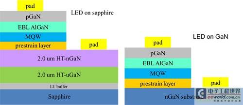
Figure 12 Schematic diagram of LED on sapphire (left) and LED on GaN (right)
Although GaN on GaN has many advantages, it is still limited by the disadvantage of the expensive substrate price, which makes it impossible to commercialize it in large quantities and raises the entry threshold for manufacturers. Therefore, the timing of entering the overall market will depend on the price reduction speed of upstream substrate manufacturers. Fortunately, thanks to the technological breakthroughs of various substrate manufacturers, more and more manufacturers are able to produce and provide gallium nitride substrates, and the time for GaN on GaN will come earlier.
From a technical perspective, LED on Sapphire has been developed for more than 10 years, accumulating considerable experience and structure, and has launched many commercial products. In contrast, GaN on GaN is still in the laboratory stage. In the future commercialization process, there are still many bottlenecks to overcome. From a technical perspective, these include the dissolution rate of aluminum and indium, the activation rate of silicon and magnesium doping; the structural changes caused by substrate defects and reduced polarization field of each epitaxial layer; the ohmic contact problem of Ga-face and N-face caused by N-type doping of the substrate; and the problem of grain grinding and cutting caused by residual internal stress of the substrate itself, etc., which still require the research team to devote efforts to solve.
GaN on GaN has great potential for development
Currently, ITRI has successfully established a high-temperature atmospheric pressure epitaxy machine and has been working on GaN on GaN technology for many years, from the early HVPE gallium nitride substrate to the current blue-violet LED epitaxy technology, and the technology has surpassed the efficiency of the current GaN on Sapphire. In the future, from the perspective of cost, by shortening the time of epitaxy and baking chamber, reducing the cost of chamber maintenance, the advantage of high current operation and the production cost of vertical structure, etc., combined with the trend of decreasing cost of gallium nitride substrate, GaN on GaN will be a rising star with great potential.
Previous article:High-performance LED spotlight solution based on TRUEC2 patented technology
Next article:Implementation of Visible Light Communication on Outdoor LED Street Lights
- Popular Resources
- Popular amplifiers
- MathWorks and NXP Collaborate to Launch Model-Based Design Toolbox for Battery Management Systems
- STMicroelectronics' advanced galvanically isolated gate driver STGAP3S provides flexible protection for IGBTs and SiC MOSFETs
- New diaphragm-free solid-state lithium battery technology is launched: the distance between the positive and negative electrodes is less than 0.000001 meters
- [“Source” Observe the Autumn Series] Application and testing of the next generation of semiconductor gallium oxide device photodetectors
- 采用自主设计封装,绝缘电阻显著提高!ROHM开发出更高电压xEV系统的SiC肖特基势垒二极管
- Will GaN replace SiC? PI's disruptive 1700V InnoMux2 is here to demonstrate
- From Isolation to the Third and a Half Generation: Understanding Naxinwei's Gate Driver IC in One Article
- The appeal of 48 V technology: importance, benefits and key factors in system-level applications
- Important breakthrough in recycling of used lithium-ion batteries
- LED chemical incompatibility test to see which chemicals LEDs can be used with
- Application of ARM9 hardware coprocessor on WinCE embedded motherboard
- What are the key points for selecting rotor flowmeter?
- LM317 high power charger circuit
- A brief analysis of Embest's application and development of embedded medical devices
- Single-phase RC protection circuit
- stm32 PVD programmable voltage monitor
- Introduction and measurement of edge trigger and level trigger of 51 single chip microcomputer
- Improved design of Linux system software shell protection technology
- What to do if the ABB robot protection device stops
- CGD and Qorvo to jointly revolutionize motor control solutions
- CGD and Qorvo to jointly revolutionize motor control solutions
- Keysight Technologies FieldFox handheld analyzer with VDI spread spectrum module to achieve millimeter wave analysis function
- Infineon's PASCO2V15 XENSIV PAS CO2 5V Sensor Now Available at Mouser for Accurate CO2 Level Measurement
- Advanced gameplay, Harting takes your PCB board connection to a new level!
- Advanced gameplay, Harting takes your PCB board connection to a new level!
- A new chapter in Great Wall Motors R&D: solid-state battery technology leads the future
- Naxin Micro provides full-scenario GaN driver IC solutions
- Interpreting Huawei’s new solid-state battery patent, will it challenge CATL in 2030?
- Are pure electric/plug-in hybrid vehicles going crazy? A Chinese company has launched the world's first -40℃ dischargeable hybrid battery that is not afraid of cold
- [Atria Development Board AT32F421 Review] - Experience Sharing
- MCU newbie asks for help regarding data transfer instructions
- MATLAB's UDP communication - How to send large batches of data packets via MATLAB's UDP
- [Blood Oximeter] Disassembly Part 4 Product Trial
- A P-MOS driving circuit
- DS18B20 Digital Temperature Sensor
- Static electricity
- How to create a schematic symbol with many pins?
- EEWORLD University - How to perform frequency response analysis on an oscilloscope
- 【NUCLEO-L552ZE Review】-2: Stay in TrustZone

 LM614IWMX


 京公网安备 11010802033920号