With the application of LED lights in many fields, such as commercial lighting and home lighting, LED lighting has completely replaced traditional incandescent lamps and fluorescent lamps. Compared with traditional lighting, LED lighting is more expensive, but it has significant advantages such as energy saving, high light efficiency, long life, and no pollution. Therefore, LED lighting can be recognized by the market in a short time. In addition, with the uncontrolled consumption of energy resources, lighting products with energy-saving performance have been promoted by government organizations, and energy organizations in some countries have also issued relevant policies to subsidize lighting products that meet their standards. For example, the power factor of commercial lighting products is greater than 0.9, and that of household lighting is greater than 0.7, which is one of the mandatory requirements of the US Energy Star. Therefore, while paying attention to the high light efficiency and long life of LED lamps, it is particularly important to design a high power factor and high performance and reliable LED driver solution under the premise of ensuring low component costs.
1 Overview of the development of LED lighting
It is considered that consumers are switching from traditional lighting to LED lighting. An article points out that LED lighting can save 80% of energy compared to incandescent lamps, and its life span can be as long as 10-20 years. In addition, compared with compact energy-saving lamps, LED lamps do not contain substances that are harmful to the environment, such as mercury and other heavy metals, and do not have the problem of long warm-up time when starting up like energy-saving lamps (CFL). Therefore, in the context of global resource shortages, in order to balance the relationship between the environment and energy, policies will also accelerate the promotion of LED lighting, because LED lighting is far superior to traditional lighting products in terms of luminous principles, energy saving, and environmental protection. Although the cost of LED lighting is very high in a short period of time, for example, the retail price of a traditional 60W incandescent lamp is less than 1/10 of that of a 7W LED lamp, so the price tolerance of household users for LED lamps is still limited at this stage, but on the other hand, in most of the newly built commercial lighting markets, such as hotels and shopping malls, LED lighting is used, and there is rarely any trace of traditional lighting.
This article will mainly discuss the driver part of LED lighting, how to reduce input current harmonics and improve input power factor. Developed countries have paid great attention to energy issues in the field of lighting. For example, the European energy standard EVP5 and the US Energy Star have clearly stipulated that the power factor PF of residential lighting drivers must be greater than 0.7 and that of commercial lighting must be greater than 0.9.
2 Buck LED Driver
2.1 Introduction to Buck LED Drivers
The three commonly used basic power conversion structures usually refer to buck, boost and buck-boost structures. They are all non-isolated, and the input and output voltages are connected to the same ground line. Each structure has its own characteristics, such as static voltage conversion rate, input-output current characteristics, output voltage ripple and the most important frequency response characteristics. The most common and simplest structure is the buck structure. The buck structure is usually chosen during design because the output voltage on the LED is always less than the input voltage, and a non-isolated structure can be used. Here is another feature of the buck structure. Because the current of the main switch tube rises from zero to the rated value in each switching cycle, its input current is always discontinuous, while the output current is continuous. This is because the output current is provided by the inductor and the capacitor at the output end.
In actual LED driver design, a buck structure is used for medium and high LED voltage outputs because it is not only simple in structure but also has obvious advantages in component cost and conversion efficiency, so it is widely used.

Figure 2.1: Step-down structure circuit diagram and test values
Figure 2.1 is a conventional BUCK step-down circuit. The chip is NXP's SSL2109 controller. It can be seen from the schematic diagram that it has very few peripheral components and a very simple circuit. The inductor only needs one winding, unlike other controllers that must rely on another auxiliary winding to power the chip. Here it uses a high-voltage ceramic capacitor C5, connected to the main switch gate for charging, so after the chip is started, the normal working level comes from the effect of this capacitor. In terms of efficiency, it can reach more than 90%, but the disadvantage is that the power factor is only about 0.55, as shown in the curve on the right side of Figure 2.1.
2.2 Working Principle of Buck LED Driver
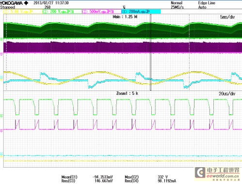
The main operating waveforms of the buck circuit are shown in Figure 2.2. The purple channel is the current waveform between the drain and source of the main switch tube Q1, the green channel is the drain voltage waveform of the main switch tube Q1, the blue channel is the input current waveform, and the yellow channel is the input voltage waveform.

Figure 2.2: Step-down structure test waveform
It can be seen that the average value of the current flowing through the main switch tube is basically a horizontal line. The main reason is that the capacity of the filter capacitor (C1, C2) after rectification is very large. The storage voltage after it is fully charged is sufficient to be discharged in the entire cycle, so the input voltage will always be higher than the output voltage. The current flowing through the switch tube in each cycle is converted into a voltage signal through resistor R5 and compared with the chip pin 4 detection. Generally, the level of the current reference pin inside the chip is a fixed value, usually around 0.5V. When the reference value is reached, the main switch tube stops working and waits for the next turn-on signal. That is, when the lowest valley voltage on the switch tube is detected, the chip provides a turn-on drive signal to the gate of the main switch tube. Therefore, the current size of the switch tube in each cycle is basically the same, which also causes the change of the current on the input line (the light blue channel in Figure 2.2) not to change with the change of the input voltage (the yellow channel in Figure 2.2). Therefore, in this design, the input power factor will be very low and the current harmonics will be very large.
3 Valley-fill LED Driver
3.1 Principle of Power Factor Correction in Valley-Fill Structure
In order to meet the requirements of Energy Star and IEC (International Electrotechnical Commission), most designers used passive valley filling to improve the input power factor in the early stage. The general circuit structure is shown in Figure 3.1 below:

Figure 3.1: Valley-filling circuit diagram and simulation results. Components C1, D5, C2, D7, and D6 form the main valley-filling circuit. In each cycle, the AC is rectified by bridge stacks D1~D4 and charged in series with C1 and C2. D6 prevents C2 from discharging back through C1. The full charge of C1 and C2 is discharged in parallel through D7 and D5. The right side of Figure 3 is the simulation result of the input current of the circuit. It can be observed that the input line current of each cycle changes continuously from 30° to 150°, 210°, and 330°, and changes discontinuously from 150° to 210° and 330° to 360°. Most of the current distortion occurs during these discontinuous times. If these distortions are reduced, the harmonic performance will be further improved. The simulation diagram shows that there is a high current spike in each positive and negative cycle, which is also one of the factors causing current distortion. This spike can be suppressed by other components, but in high-power applications, it is necessary to balance the efficiency and heat issues.
3.2 Experimental test of power factor of valley-filling drive
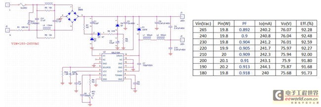
The passive valley-filling circuit introduced above is added to the conventional BUCK structure. The components here are C1, C2, D2, D3, D4 and R2. Resistor R2 can help improve the harmonic current and reduce the maximum current peak in the simulation results of Figure 3.1. In the experiment, the main control buck chip uses NXP's SSL21084 product. SSL21084 only integrates the main switch tube into the chip. The switch control method is exactly the same as SSL2109. The specific circuit is shown in Figure 3.2-1:

Figure 3.2-1: Valley-filling buck structure circuit and test results
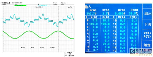
The right side of Figure 3.2-1 is the test result of a 20W LED driver. After using a passive valley-filling circuit, when the input voltage changes from 200V to 265V, the power factor PF has been increased from the original 0.6 to more than 0.9, and the efficiency can reach 92%. Therefore, while the power factor is improved, the efficiency has not been significantly reduced. Figure 3.2-2 is the waveform of the input voltage and input current. The green channel is the input voltage waveform, and the light blue channel is the input current waveform. It is obvious that although the power factor has been improved, the input current waveform is still distorted, so the total harmonic factor is not very good. The test data shows that the total current harmonic is 38%. As shown in the harmonic test data on the right side of Figure 3.2-2, the 3rd, 5th, 7th, and 9th odd harmonic values are still very high.

Figure 3.2-2: Valley-filling buck structure test waveform and harmonic results
4 Active LED Driver
Methods and characteristics of active power factor correction
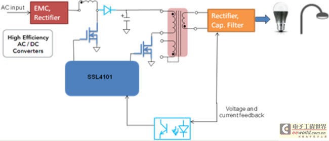
Active power factor correction is usually implemented using a bipolar topology, with a boost circuit structure in the front stage and an isolated flyback structure in the back stage DC conversion part, as shown in Figure 4.1. The power factor correction chip uses the SSL4101 controller of NXP Semiconductors, which operates in critical conduction mode and constant conduction time control. The current flowing through the inductor is proportional to the voltage after the bridge rectifier, so the phase of the input average current will follow the input voltage, resulting in a very high power factor. This control loop has high reliability and is often used in medium and high power drivers. SSL4101 also integrates flyback conversion control function. For example, quasi-resonant discontinuous control is often used. The characteristic of quasi-resonant operation is to ensure that the voltage on the parasitic capacitor on the main switch is turned on when it drops to the minimum, reducing switching losses and helping electromagnetic radiation to a certain extent. The voltage and current levels of the secondary output are fed back to the primary controller through an optocoupler (abbreviated as optocoupler). Compared with the valley-fill structure, the active power factor correction design can achieve higher power factor and lower harmonic current, and the output LED current ripple is also very low. However, the drive design of this two-stage structure is very complex, and the component cost is also very high. It is generally only suitable for use in LED drivers with power greater than 75W.

Figure 4: Two-stage active power factor correction structure diagram
Previous article:Popularization of basic knowledge of LED
Next article:Design of high power factor driver for LED lamp (Part 2)
Recommended ReadingLatest update time:2024-11-16 16:19


- Popular Resources
- Popular amplifiers
-
 Siemens Motion Control Technology and Engineering Applications (Tongxue, edited by Wu Xiaojun)
 -
 Modern Product Design Guide
 -
 Modern arc welding power supply and its control
 -
 Small AC Servo Motor Control Circuit Design (by Masaru Ishijima; translated by Xue Liang and Zhu Jianjun, by Masaru Ishijima, Xue Liang, and Zhu Jianjun)
- MathWorks and NXP Collaborate to Launch Model-Based Design Toolbox for Battery Management Systems
- STMicroelectronics' advanced galvanically isolated gate driver STGAP3S provides flexible protection for IGBTs and SiC MOSFETs
- New diaphragm-free solid-state lithium battery technology is launched: the distance between the positive and negative electrodes is less than 0.000001 meters
- [“Source” Observe the Autumn Series] Application and testing of the next generation of semiconductor gallium oxide device photodetectors
- 采用自主设计封装,绝缘电阻显著提高!ROHM开发出更高电压xEV系统的SiC肖特基势垒二极管
- Will GaN replace SiC? PI's disruptive 1700V InnoMux2 is here to demonstrate
- From Isolation to the Third and a Half Generation: Understanding Naxinwei's Gate Driver IC in One Article
- The appeal of 48 V technology: importance, benefits and key factors in system-level applications
- Important breakthrough in recycling of used lithium-ion batteries
- Innolux's intelligent steer-by-wire solution makes cars smarter and safer
- 8051 MCU - Parity Check
- How to efficiently balance the sensitivity of tactile sensing interfaces
- What should I do if the servo motor shakes? What causes the servo motor to shake quickly?
- 【Brushless Motor】Analysis of three-phase BLDC motor and sharing of two popular development boards
- Midea Industrial Technology's subsidiaries Clou Electronics and Hekang New Energy jointly appeared at the Munich Battery Energy Storage Exhibition and Solar Energy Exhibition
- Guoxin Sichen | Application of ferroelectric memory PB85RS2MC in power battery management, with a capacity of 2M
- Analysis of common faults of frequency converter
- In a head-on competition with Qualcomm, what kind of cockpit products has Intel come up with?
- Dalian Rongke's all-vanadium liquid flow battery energy storage equipment industrialization project has entered the sprint stage before production
- Allegro MicroSystems Introduces Advanced Magnetic and Inductive Position Sensing Solutions at Electronica 2024
- Car key in the left hand, liveness detection radar in the right hand, UWB is imperative for cars!
- After a decade of rapid development, domestic CIS has entered the market
- Aegis Dagger Battery + Thor EM-i Super Hybrid, Geely New Energy has thrown out two "king bombs"
- A brief discussion on functional safety - fault, error, and failure
- In the smart car 2.0 cycle, these core industry chains are facing major opportunities!
- The United States and Japan are developing new batteries. CATL faces challenges? How should China's new energy battery industry respond?
- Murata launches high-precision 6-axis inertial sensor for automobiles
- Ford patents pre-charge alarm to help save costs and respond to emergencies
- New real-time microcontroller system from Texas Instruments enables smarter processing in automotive and industrial applications
- Video explains the triggering modes of oscilloscopes and what they mean
- 【EasyARM-RT1052 Review】 + LWIP transplantation and use
- Comic Science: The Principle of Antenna
- Design of Network Camera Based on TMS320DM642
- EEWORLD University Hall----Introduction to Computer Vision
- Has anyone used STM8L151K4T6? Is the DAC of this chip stable?
- My thoughts
- Qorvo's RF front-end technology innovation leads the development of 5G terminals
- The official website CC2541SDK cannot print via serial port
- Why does dsp use BIOS?

 Siemens Motion Control Technology and Engineering Applications (Tongxue, edited by Wu Xiaojun)


 京公网安备 11010802033920号