With the application of LED lights in many fields, such as commercial lighting and home lighting, LED lighting has completely replaced traditional incandescent lamps and fluorescent lamps. Compared with traditional lighting, LED lighting is more expensive, but it has significant advantages such as energy saving, high light efficiency, long life, and no pollution. Therefore, LED lighting can be recognized by the market in a short time. In addition, with the uncontrolled consumption of energy resources, lighting products with energy-saving performance have been promoted by government organizations, and energy organizations in some countries have also issued relevant policies to subsidize lighting products that meet their standards. For example, the power factor of commercial lighting products is greater than 0.9, and that of household lighting is greater than 0.7, which is one of the mandatory requirements of the US Energy Star. Therefore, while paying attention to the high light efficiency and long life of LED lamps, it is particularly important to design a high power factor and high performance and reliable LED driver solution under the premise of ensuring low component costs.
1 Overview of the development of LED lighting
It is considered that consumers are switching from traditional lighting to LED lighting. An article points out that LED lighting can save 80% of energy compared to incandescent lamps, and its life span can be as long as 10-20 years. In addition, compared with compact energy-saving lamps, LED lamps do not contain substances that are harmful to the environment, such as mercury and other heavy metals, and do not have the problem of long warm-up time when starting up like energy-saving lamps (CFL). Therefore, in the context of global resource shortages, in order to balance the relationship between the environment and energy, policies will also accelerate the promotion of LED lighting, because LED lighting is far superior to traditional lighting products in terms of luminous principles, energy saving, and environmental protection. Although the cost of LED lighting is very high in a short period of time, for example, the retail price of a traditional 60W incandescent lamp is less than 1/10 of that of a 7W LED lamp, so the price tolerance of household users for LED lamps is still limited at this stage, but on the other hand, in most of the newly built commercial lighting markets, such as hotels and shopping malls, LED lighting is used, and there is rarely any trace of traditional lighting.
This article will mainly discuss the driver part of LED lighting, how to reduce input current harmonics and improve input power factor. Developed countries have paid great attention to energy issues in the field of lighting. For example, the European energy standard EVP5 and the US Energy Star have clearly stipulated that the power factor PF of residential lighting drivers must be greater than 0.7 and that of commercial lighting must be greater than 0.9.
2 Buck LED Driver
2.1 Introduction to Buck LED Drivers
The three commonly used basic power conversion structures usually refer to buck, boost and buck-boost structures. They are all non-isolated, and the input and output voltages are connected to the same ground line. Each structure has its own characteristics, such as static voltage conversion rate, input-output current characteristics, output voltage ripple and the most important frequency response characteristics. The most common and simplest structure is the buck structure. The buck structure is usually chosen during design because the output voltage on the LED is always less than the input voltage, and a non-isolated structure can be used. Here is another feature of the buck structure. Because the current of the main switch tube rises from zero to the rated value in each switching cycle, its input current is always discontinuous, while the output current is continuous. This is because the output current is provided by the inductor and the capacitor at the output end.
In actual LED driver design, a buck structure is used for medium and high LED voltage outputs because it is not only simple in structure but also has obvious advantages in component cost and conversion efficiency, so it is widely used.

Figure 2.1: Step-down structure circuit diagram and test values
Figure 2.1 is a conventional BUCK step-down circuit. The chip is NXP's SSL2109 controller. It can be seen from the schematic diagram that it has very few peripheral components and a very simple circuit. The inductor only needs one winding, unlike other controllers that must rely on another auxiliary winding to power the chip. Here it uses a high-voltage ceramic capacitor C5, connected to the main switch gate for charging, so after the chip is started, the normal working level comes from the effect of this capacitor. In terms of efficiency, it can reach more than 90%, but the disadvantage is that the power factor is only about 0.55, as shown in the curve on the right side of Figure 2.1.
2.2 Working Principle of Buck LED Driver
The main operating waveforms of the buck circuit are shown in Figure 2.2. The purple channel is the current waveform between the drain and source of the main switch tube Q1, the green channel is the drain voltage waveform of the main switch tube Q1, the blue channel is the input current waveform, and the yellow channel is the input voltage waveform.
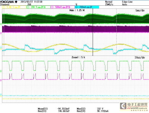
Figure 2.2: Step-down structure test waveform
It can be seen that the average value of the current flowing through the main switch tube is basically a horizontal line. The main reason is that the capacity of the filter capacitor (C1, C2) after rectification is very large. The storage voltage after it is fully charged is sufficient to be discharged in the entire cycle, so the input voltage will always be higher than the output voltage. The current flowing through the switch tube in each cycle is converted into a voltage signal through resistor R5 and compared with the chip pin 4 detection. Generally, the level of the current reference pin inside the chip is a fixed value, usually around 0.5V. When the reference value is reached, the main switch tube stops working and waits for the next turn-on signal. That is, when the lowest valley voltage on the switch tube is detected, the chip provides a turn-on drive signal to the gate of the main switch tube. Therefore, the current size of the switch tube in each cycle is basically the same, which also causes the change of the current on the input line (the light blue channel in Figure 2.2) not to change with the change of the input voltage (the yellow channel in Figure 2.2). Therefore, in this design, the input power factor will be very low and the current harmonics will be very large.
3 Valley-fill LED Driver
3.1 Principle of Power Factor Correction in Valley-Fill Structure
In order to meet the requirements of Energy Star and IEC (International Electrotechnical Commission), most designers used passive valley filling to improve the input power factor in the early stage. The general circuit structure is shown in Figure 3.1 below:

Figure 3.1: Valley-filling structure circuit diagram and simulation results
Components C1, D5, C2, D7, and D6 form the main valley filling circuit. In each cycle, the AC power is rectified by the bridge stack D1~D4, and then charged in series to C1 and C2. D6 prevents C2 from discharging through C1. The full charge of C1 and C2 is discharged in parallel through D7 and D5. The right side of Figure 3 is the simulation result of the circuit input current. It can be observed that the input line current of each cycle changes continuously from 30° to 150°, 210°, and 330°, and changes discontinuously from 150° to 210° and 330° to 360°. Most of the current distortion occurs during these discontinuous times. If these distortions are reduced, the harmonic performance will be further improved. The simulation diagram shows that there is a high current spike in each positive and negative cycle, which is also one of the factors causing current distortion. This spike can be suppressed by other components, but in high-power applications, it is necessary to balance the efficiency and heat issues.
3.2 Experimental test of power factor of valley-filling drive
The passive valley-filling circuit introduced above is added to the conventional BUCK structure. The components here are C1, C2, D2, D3, D4 and R2. Resistor R2 can help improve the harmonic current and reduce the maximum current peak in the simulation results of Figure 3.1. In the experiment, the main control buck chip uses NXP's SSL21084 product. SSL21084 only integrates the main switch tube into the chip. The switch control method is exactly the same as SSL2109. The specific circuit is shown in Figure 3.2-1:
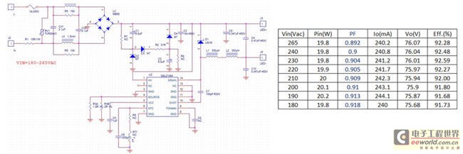
Figure 3.2-1: Valley-filling buck structure circuit and test results
The right side of Figure 3.2-1 is the test result of a 20W LED driver. After using a passive valley-filling circuit, when the input voltage changes from 200V to 265V, the power factor PF has been increased from the original 0.6 to more than 0.9, and the efficiency can reach 92%. Therefore, while the power factor is improved, the efficiency has not been significantly reduced. Figure 3.2-2 is the waveform of the input voltage and input current. The green channel is the input voltage waveform, and the light blue channel is the input current waveform. It is obvious that although the power factor has been improved, the input current waveform is still distorted, so the total harmonic factor is not very good. The test data shows that the total current harmonic is 38%. As shown in the harmonic test data on the right side of Figure 3.2-2, the 3rd, 5th, 7th, and 9th odd harmonic values are still very high.
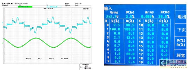
Figure 3.2-2: Valley-filling buck structure test waveform and harmonic results
4 Active LED Driver
Methods and characteristics of active power factor correction
Active power factor correction is usually implemented using a bipolar topology, with a boost circuit structure in the front stage and an isolated flyback structure in the back stage DC conversion part, as shown in Figure 4.1. The power factor correction chip uses the SSL4101 controller of NXP Semiconductors, which operates in critical conduction mode and constant conduction time control. The current flowing through the inductor is proportional to the voltage after the bridge rectifier, so the phase of the input average current will follow the input voltage, resulting in a very high power factor. This control loop has high reliability and is often used in medium and high power drivers. SSL4101 also integrates flyback conversion control function. For example, quasi-resonant discontinuous control is often used. The characteristic of quasi-resonant operation is to ensure that the voltage on the parasitic capacitor on the main switch is turned on when it drops to the minimum, reducing switching losses and helping electromagnetic radiation to a certain extent. The voltage and current levels of the secondary output are fed back to the primary controller through an optocoupler (abbreviated as optocoupler). Compared with the valley-fill structure, the active power factor correction design can achieve higher power factor and lower harmonic current, and the output LED current ripple is also very low. However, the drive design of this two-stage structure is very complex, and the component cost is also very high. It is generally only suitable for use in LED drivers with power greater than 75W.
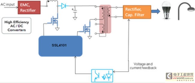
Figure 4: Two-stage active power factor correction structure diagram
5 Single-stage power factor corrected LED driver
5.1 Reasons for using single-stage power factor correction
Whether the valley filling method or active power factor correction technology is used to improve the power factor, each has its own advantages and disadvantages. For example, the valley filling circuit requires the use of high-voltage electrolytic capacitors with large capacitance, which has led to certain limitations in the design of compact LED lamps in terms of component cost and size. Although the two-stage active structure can achieve the best power factor and harmonic performance, the power factor correction circuit structure is relatively complex, which increases the cost and volume of the power supply. As a result, a single-stage power factor correction technology has been developed. Its topology is to merge and reuse the switching elements in the power factor correction circuit and the switching elements of the subsequent DC-DC converter, combining the two circuits into one. Therefore, the single-stage power factor converter has the following advantages: 1) The number of switching devices is reduced, and the volume and cost of the main circuit can be reduced; 2) The control circuit usually has only one output loop, which simplifies the control loop; 3) In the single-stage converter topology, part of the energy can be directly transferred to the output side without two-stage conversion, so the efficiency is higher than that of the two-stage converter. Due to the above characteristics, the single-stage power factor correction circuit has obvious advantages in small and medium-power LED drivers.
5.2 Working Principle of Single-Stage Buck Power Factor Correction
The main reason why the power factor in the traditional buck structure is too low has been mentioned above. So here we need to solve the problem of how to adjust the average current flowing through the main switch tube to be close to the phase of the voltage change, that is, in each cycle, let the current change with the voltage change, so as to achieve the purpose of high power factor.
The circuit shown in Figure 5.2 is a simulation diagram of the peripheral control circuit used to adjust the main switch current. The circuit principle is to obtain a frequency twice that of the AC power at the emitter end of the transistor Q1, which is close to a half-sine wave. This level is then provided to the current feedback pin of the control chip SSL2109. The chip then modulates the main circuit operating frequency so that the average current flowing through the main switch tube forms a shape that is approximately half-sine.
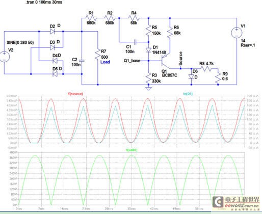
Figure 5.2: Single-stage power factor adjustment circuit simulation diagram
The curve part below Figure 5.2 is the result of simulation. The green curve is the voltage shape after bridge rectification. The red curve and the blue curve are the results of the collector voltage and current of the transistor Q1 respectively. It can be seen that the base level of the transistor completely follows the voltage after bridge rectification. Since the transistor Q1 is a PNP transistor, the level of the collector output is just opposite to the level of the base-emitter. Therefore, when the base level decreases from the highest amplitude to zero, the collector output voltage and current gradually increase from the lowest to the highest amplitude. In this way, when this level is input to the current feedback pin of the chip, the current of the main switch tube can be adjusted.
5.3 Verification of single-stage power factor adjustment circuit in buck structure
Figure 5.3-1 adds a power factor adjustment element to the traditional BUCK step-down circuit, so the signal detected by the chip current foot is the sum of the main switch tube M1 and the current flowing through the transistor Q1. When the rectified voltage changes, the current flowing through the transistor Q1 also changes.

Figure 5.3-1: Single-stage power factor adjustment test diagram and related test waveforms
The right side of Figure 5.3-1 shows the working waveform obtained by testing on the experimental board. From top to bottom, the channels are: purple is the voltage waveform of the gate of the main switch tube, the dark blue channel is the waveform of the chip current detection pin, the green channel is the current waveform on the source of the main switch tube M1, and the light blue channel is the waveform of the input current. It can be seen that the chip current detection pin was originally a constant 0.5 reference level. Now, after using the external power factor correction circuit, the average current waveform of the main switch is adjusted to a semi-sine shape. The reason is that after the output level of the collector of the triode Q1 enters the chip current detection pin, the current on the main switch tube will first gradually increase from the zero point to the maximum amplitude, and then gradually decrease to zero. In this way, the phases of the input current and input voltage are basically similar, and are also close to the AC sine.
Figure 5.3-2 shows the result of the total current harmonic test obtained in the experiment, which is only 13%. It can be seen that compared with the original buck and valley-filling buck, there is a significant improvement, which fully meets the power factor requirements of Energy Star for LED lighting. The inductor selected in this experiment is EFD15, with an inductance of 700mH, a minimum operating frequency of 70KHz, a power factor of 0.95, and a working efficiency of more than 93%.
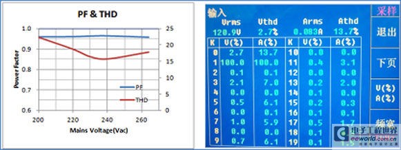
Figure 5.3-2: Single-stage power factor adjustment test results
Figure 5.3-1 compares the original step-down structure circuit diagram 2.1, and there are also improvements in the open circuit protection of LED lamps. The original diagram uses a voltage regulator and a thyristor with a large power rating to protect the output voltage from being too high and causing damage to the output electrolytic capacitor. The disadvantage is that when an open circuit occurs, the main chip is always working and does not stop. The temperature of the thyristor used for protection will also be relatively high, which has certain safety hazards. In Figure 10, only a winding is added to the inductor to sense the change of the output voltage. The diode D2 rectifies the negative voltage of the newly added winding. When the LED lamp is open, the voltage across the electrolytic capacitor C1 rises, and the absolute voltage of the newly added winding will also increase. The negative voltage rectified by D2 will also increase until the voltage regulator D4 is turned on, thereby pulling the chip NTC pin level down to 0V, the main switch stops working, and the chip enters the protection mode. Therefore, this open circuit protection is simpler and more reliable than the original protection.
5.4 Verifying a single-stage power factor adjustment circuit in a flyback structure
Of course, the peripheral circuit of power factor correction in the single-stage buck structure can also be used in the isolated flyback structure, because in some LED lighting, the design requirements of the isolated flyback structure are also very high. Figure 5.4 is the test data of the isolated flyback structure. The control chip still uses NXP's SSL2109. From the test results, we can see that the power factor and harmonic current are basically the same as those in the buck structure, and both can achieve a power factor (PF) value greater than 0.9 and a harmonic current less than 20%.
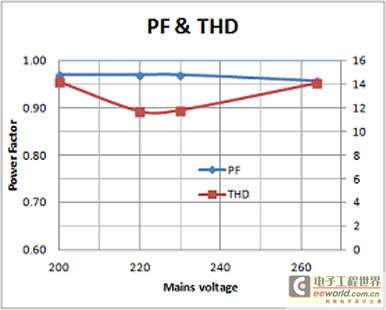
Figure 5.4: Power factor adjustment circuit in flyback structure application results
6 Conclusion
6.1 Summarize and compare the characteristics of three power factor correction methods
In the previous section, we introduced the three power factor correction structures and conducted related experiments. It can be seen that each structure has its own characteristics. Table 6.1 compares the three power factor correction methods. The active power factor correction flyback conversion structure has the best power factor and harmonic performance, but its disadvantage is that the circuit complexity and component cost are higher than the other two. The disadvantage of the valley-filling power correction structure is that the power factor is not high enough and the harmonic performance is still not good. Although the component cost is lower than that of the active structure, it is still higher than that of the unipolar structure. The single-stage power factor correction structure can fully meet the requirements of IEC63000-3-2 in terms of harmonic and power factor performance. Its power factor adjustment method is not only simple in structure, but also has the lowest cost of peripheral components. On the other hand, in the single-stage adjustment structure, because the filter capacitor capacity after bridge rectification is very small, generally around 100~200nF, the low-frequency ripple of the output current will be larger than that of the previous two structures, but this problem can be solved by increasing the output capacitor capacity.

Table 6.1: Performance comparison results of three power factor correction methods
6.2 Conclusion:
This paper discusses and studies the design of LED lighting drivers, especially how to obtain high power factor and low current harmonic performance with low cost methods. After theoretical analysis and practical experimental demonstration, it is proved that the single-stage power factor adjustment structure improved on the traditional buck structure can fully achieve high power factor and low harmonic performance, and can also be easily applied to the actual design of LED lighting drivers.
Previous article:Tips for Correctly Choosing LED Driver Power Supply
Next article:LED driver chip selection
- Popular Resources
- Popular amplifiers
- MathWorks and NXP Collaborate to Launch Model-Based Design Toolbox for Battery Management Systems
- STMicroelectronics' advanced galvanically isolated gate driver STGAP3S provides flexible protection for IGBTs and SiC MOSFETs
- New diaphragm-free solid-state lithium battery technology is launched: the distance between the positive and negative electrodes is less than 0.000001 meters
- [“Source” Observe the Autumn Series] Application and testing of the next generation of semiconductor gallium oxide device photodetectors
- 采用自主设计封装,绝缘电阻显著提高!ROHM开发出更高电压xEV系统的SiC肖特基势垒二极管
- Will GaN replace SiC? PI's disruptive 1700V InnoMux2 is here to demonstrate
- From Isolation to the Third and a Half Generation: Understanding Naxinwei's Gate Driver IC in One Article
- The appeal of 48 V technology: importance, benefits and key factors in system-level applications
- Important breakthrough in recycling of used lithium-ion batteries
- LED chemical incompatibility test to see which chemicals LEDs can be used with
- Application of ARM9 hardware coprocessor on WinCE embedded motherboard
- What are the key points for selecting rotor flowmeter?
- LM317 high power charger circuit
- A brief analysis of Embest's application and development of embedded medical devices
- Single-phase RC protection circuit
- stm32 PVD programmable voltage monitor
- Introduction and measurement of edge trigger and level trigger of 51 single chip microcomputer
- Improved design of Linux system software shell protection technology
- What to do if the ABB robot protection device stops
- Keysight Technologies Helps Samsung Electronics Successfully Validate FiRa® 2.0 Safe Distance Measurement Test Case
- Innovation is not limited to Meizhi, Welling will appear at the 2024 China Home Appliance Technology Conference
- Innovation is not limited to Meizhi, Welling will appear at the 2024 China Home Appliance Technology Conference
- Huawei's Strategic Department Director Gai Gang: The cumulative installed base of open source Euler operating system exceeds 10 million sets
- Download from the Internet--ARM Getting Started Notes
- Learn ARM development(22)
- Learn ARM development(21)
- Learn ARM development(20)
- Learn ARM development(19)
- Learn ARM development(14)
- If you are interested in AI, which technology do you focus on?
- [EVAL-M3-TS6-665PN] Interpretation again
- What is output impedance? What is impedance matching?
- [Unboxing and document display of the ACM32F070 capacitive touch development board]
- Importance of CMTI parameter for isolation driver selection
- Gold - Sand - Wafers - Artwork - Qorvo Semiconductor
- Programmable sensor-specific detection MCU CS88F313
- [National Technology N32G457 Review] 4. PWM and breathing light test
- How to make a jumper between the pads of two different plug-ins in PCB?
- "Core" ecosystem, "Assist" security, "Connect" the future. Registration for the 2021 STM32 China Summit and Fan Carnival is now open!

 AD822ARM-REEL7


 京公网安备 11010802033920号