An important goal in double-pulse testing is to accurately measure energy loss. For accurate power and energy testing in an oscilloscope, the key step is to calibrate the voltage probe and current probe to eliminate timing deviations.
Double-pulse test software (WBG-DPT) can be used on 4-series, 5-series and 6-series oscilloscopes. The software includes a new calibration technology designed for double-pulse testing to eliminate timing deviation (deskew). This new method is very different from the traditional method, and the test speed is significantly accelerated and the test time is shortened.

This technology is suitable for power converters using field effect transistors or IGBTs. In this article, we will use FET terminology to keep the description simple and clear.
Why should we eliminate timing skew ( deskew )?
When designing any kind of power converter, it is necessary to minimize the energy loss during the switching process. This energy loss can be measured using an oscilloscope. The general method is to multiply the voltage and current samples at the same time to generate a power waveform.
p(t) = v(t)*i(t)
Since the power waveform represents energy consumption over time, the energy can be determined by integrating the power waveform:
E = ∫p(t)dt
To accurately measure energy loss, the transitions in current and voltage waveforms should be consistent in time. Therefore, to make accurate energy loss measurements, designers must correct for delays caused by test fixtures and probes.
Generally speaking, the deviation between probes is calculated before starting any measurement on the test setup. For low-voltage applications, calibration can be performed using a function generator and a timing skew calibration fixture (deskew fixture) (Tektronix P/N 067-1686-03). However, this approach is not optimal for high voltage and high current applications.
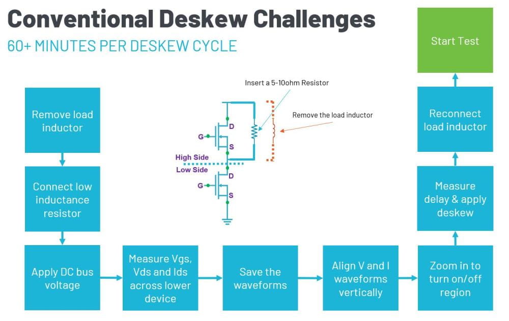
In order to match the measurement of low-voltage drain-source voltage (VDS) and drain current (ID) at higher powers, traditional techniques require rewiring the test setup. This requires removing the load inductor and replacing it with a resistor. Next, the measurements are taken and the VDS and ID measurements need to be matched. This process may take an hour or more.

A new timing skew calibration ( deskew ) method
Tektronix WBG-DPT solution is the industry's first software-based timing deviation calibration (deskew) technology that does not require rewiring and can be performed only after double-pulse measurement. In the new method, the drain current (ID) is collected and used as a reference waveform. During the turn-on period, the low-voltage side VDS alignment waveform is calculated using the parameter model of the test circuit. The calculated waveform refers to the ID waveform and has no timing offset relative to the ID. The timing skew elimination algorithm determines the timing skew between the calculated VDS waveform and the measured VDS waveform. The deskew calibrated data is then corrected to the VDS measurement channel.
Timing Skew Calibration Process
As mentioned above, timing offset calibration can be performed after measurement. There is no need to worry about the deviation between VDS and ID when starting a double pulse test, then select the deskew setting and provide the following parameters:
Probe Impedance - assumed in this article to be the current sense resistor (CVR) or shunt resistor
Effective "loop" inductance
Bias voltage (average VDS across low-side FET when turned off)
Difference order (the order of the filter used by the model for smoothing)

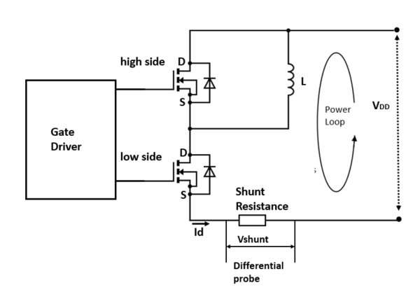
Figure 3. Equivalent circuit used to create VDS_low aligned waveforms. This circuit assumes the use of a current-sighting resistor to measure ID .
The parameters entered in the deskew menu are used to construct the VDS corresponding waveform. The waveform is built using Kirchhoff's voltage law:

in
V DD - V DS_high represents the supply rail voltage and the voltage drop across the high side field effect transistor FET. It should be noted that during turn-on, this quantity is constant since V DD is fixed and V DS_high is the voltage on the body diode of the high-side field effect transistor FET.
R shunt is the shunt resistor.
ID is the drain current measured from the voltage drop across R shunt .
dI D /dt is the measured rate of change of drain current.
L eff is the effective inductance of the entire power loop.
As mentioned above, during turn-on, V DD - V DS_high is effectively constant. R shunt and L eff are also constant. This means that the simulated V DS_low trace waveform is a function of ID .
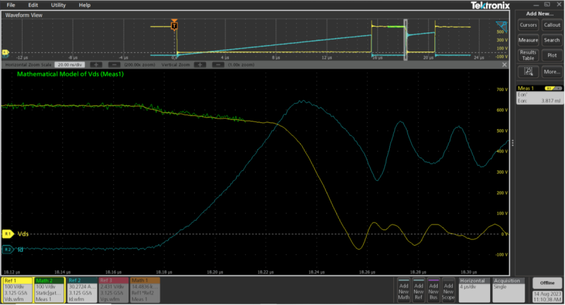
After configuring the parameters, the user presses the WBG's deskew button. The system will generate a mathematical model of VDS based on the specified parameters and drain current. The waveform will be displayed on the screen.

Figure 4. Calculated V DS alignment waveform based on ID compared to measured V DS waveform. Offset is the time difference between the aligned waveform and the measured waveform. Once the skew is calculated, it can be removed from the ID waveform .
As shown in the figure above, the effective inductance L eff takes into account the "superposition" of the entire loop. Therefore, L eff is usually unknown, and this parameter needs to be adjusted repeatedly. Simply run the correction process over and over again and adjust L eff until the calculated alignment waveform and measured V DS waveform have the same shape. If there is a difference in shape between the calculated V DS alignment waveform and the measured V DS waveform, you can adjust the parameters and run the calibration time offset again.
Once the parameters are set accurately, the alignment and measurement waveforms will have the same shape, allowing the system to identify and correct skew. The skew value is displayed in the Deskew setting and is automatically applied to the channel connected to the V DS signal.
This new process accurately calculates skew values and reduces timing skew calibration time from an hour or more to 5 to 10 minutes.
Previous article:Keysight Technologies and CTTL Complete First CTIA MIMO OTA Dynamic Channel Model Test System Validation
Next article:Loop response test using MSO6 series oscilloscope
- Popular Resources
- Popular amplifiers
- Seizing the Opportunities in the Chinese Application Market: NI's Challenges and Answers
- Tektronix Launches Breakthrough Power Measurement Tools to Accelerate Innovation as Global Electrification Accelerates
- Not all oscilloscopes are created equal: Why ADCs and low noise floor matter
- Enable TekHSI high-speed interface function to accelerate the remote transmission of waveform data
- How to measure the quality of soft start thyristor
- How to use a multimeter to judge whether a soft starter is good or bad
- What are the advantages and disadvantages of non-contact temperature sensors?
- In what situations are non-contact temperature sensors widely used?
- How non-contact temperature sensors measure internal temperature
- LED chemical incompatibility test to see which chemicals LEDs can be used with
- Application of ARM9 hardware coprocessor on WinCE embedded motherboard
- What are the key points for selecting rotor flowmeter?
- LM317 high power charger circuit
- A brief analysis of Embest's application and development of embedded medical devices
- Single-phase RC protection circuit
- stm32 PVD programmable voltage monitor
- Introduction and measurement of edge trigger and level trigger of 51 single chip microcomputer
- Improved design of Linux system software shell protection technology
- What to do if the ABB robot protection device stops
- CGD and Qorvo to jointly revolutionize motor control solutions
- CGD and Qorvo to jointly revolutionize motor control solutions
- Keysight Technologies FieldFox handheld analyzer with VDI spread spectrum module to achieve millimeter wave analysis function
- Infineon's PASCO2V15 XENSIV PAS CO2 5V Sensor Now Available at Mouser for Accurate CO2 Level Measurement
- Advanced gameplay, Harting takes your PCB board connection to a new level!
- Advanced gameplay, Harting takes your PCB board connection to a new level!
- A new chapter in Great Wall Motors R&D: solid-state battery technology leads the future
- Naxin Micro provides full-scenario GaN driver IC solutions
- Interpreting Huawei’s new solid-state battery patent, will it challenge CATL in 2030?
- Are pure electric/plug-in hybrid vehicles going crazy? A Chinese company has launched the world's first -40℃ dischargeable hybrid battery that is not afraid of cold
- Flash is locked and the emulator cannot connect to the chip. Error message: No target connected
- Vote: Which of these TI star products do you like?
- It was not until the PCBA could not be assembled that I realized the importance of the silk screen marking of the package design.
- How to achieve 4-20mA current isolation output of microcontroller?
- Buck-boost supercapacitor charging solution
- Temperature detection [What is the device sensor you are most comfortable using]?
- Raspberry Pico Review Summary
- JZ2440 Development Board
- EEPROM lifespan issue?
- Huawei_Static Timing Analysis and Logic Design.pdf

 UPC393G2-E2-A


 京公网安备 11010802033920号