Frequency synthesis technology is an important part of modern communication. It converts a high-stability and high-accuracy reference frequency into an arbitrary frequency with the same stability and accuracy through arithmetic operations. The frequency synthesizer is the heart of the electronic system and one of the key factors affecting the performance of the electronic system. This paper combines FPGA technology, phase-locked loop technology, and frequency synthesis technology to design an integer/half-integer frequency synthesizer, which can be easily applied to phase-locked loop teaching and has certain practical value.
1 Basic principles of PLL frequency synthesizer
Frequency synthesizers are mainly divided into four types: direct, phase-locked, direct digital, and hybrid. At present, phase-locked and digital types are easy to realize serialization, miniaturization, modularization, and engineering, and their performance is getting better and better. They have gradually become the most typical and widely used frequency synthesizers [1]. This paper mainly adopts the integrated phase-locked loop PLL phase-Lockde Loop chip CD4046 and uses FPGA to realize PLL frequency synthesizer.
Phase-locked frequency synthesizer is composed of PLL. The principle block diagram of a typical phase-locked frequency synthesizer is shown in Figure 1.

Its working process can be simply described as follows: the average DC value of the phase detector output current multiplied by the impedance of the loop filter forms the input control voltage of the VCO. The VCO is a voltage-frequency conversion device with a proportional constant. The control voltage of the loop filter adjusts the output phase of the VCO, and after dividing by N, it is equal to the phase of the comparison frequency. Because the phase is the integral of the frequency, this process also applies to the frequency. The output frequency can be expressed as:

Formula 1 is only valid when the PLL is in the locked state, and it is not valid in the intermediate process of the PLL being readjusted to the locked state. In actual applications, the R value is fixed, the N value is variable [2], and XTAL is the frequency of the input signal.
2 System Design
The functions of the entire system are mainly implemented by the FPGA chip EPF10K10 LC84-4 to control related hardware. The principle block diagram of this system is shown in Figure 2.
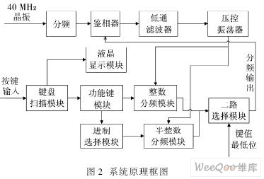
As can be seen from Figure 2, on the one hand, the 40 MHz active crystal oscillator is divided by the control of the FPGA to obtain a 1 kHz frequency signal, which is used as the input reference frequency division of the CD4046. The output signal of the VCO of the CD4046 is directly input into the integer frequency division module and the half-integer frequency division module; on the other hand, the keyboard scans and outputs the key value, which is sent to the functional module. If the functional module indicates "OK", the key value is sent as the frequency division coefficient to the integer frequency division module and the half-integer frequency division module to divide the signal input by the VCO respectively; if the functional module indicates "clear", the frequency division coefficient is cleared. The last bit of the key value directly controls the two-way selection module: if the last bit of the key value is "0", the two-way selection module is controlled to output the integer module result; if the last bit of the key value is "5", the two-way selection module is controlled to output the half-integer module result. The result of the frequency division output is compared with the reference frequency of the phase-locked loop in the phase detector, and a Ud voltage signal corresponding to the phase difference of the two signals is generated. The high-frequency components and noise in Ud are filtered out by the loop filter, and Uc is output. Uc is then input into the VCO, so that the oscillation frequency of the voltage-controlled oscillator keeps approaching the frequency of the input signal, and finally the loop is locked, and the VCO outputs a stable frequency.
During the operation, the FPGA controls the change of the preset N/N+0.5. When N/N+0.5 changes, the output signal frequency response changes with the input signal. At the same time, the FPGA also realizes the functions of keyboard scanning and LCD display.
2.1 System hardware design
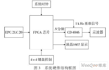
The hardware is shown in Figure 3. The system part is mainly composed of 7 parts: external system clock, 4×4 keyboard control circuit, FPGA processing chip, EPC2LC20 EPROM chip, PLL chip CD4046 and its peripheral circuit, LCD 1602 display module, oscilloscope. This design uses the FPGA dedicated configuration chip EPC2, and downloads the program to the FPGA chip multiple times through the download cable ByteBlaster MV. The system uses FPGA chip as the control center, inputs control information by key scanning, and displays it on the LCD screen. It can conveniently and intuitively demonstrate the application of PLL chip CD4046 in frequency synthesis technology, and achieve the expected index requirements. The specific models of the main hardware in this design are: LCD TC1602A-01T, FPGA chip EPF10K10LC84-4, 40.000 MHz active crystal oscillator HO-12B.
2.2 System software design
By writing VHDL program to realize integer/half-integer frequency division, and using Quartus II and ModelSim, the author completed the design and simulation of VHDL program.
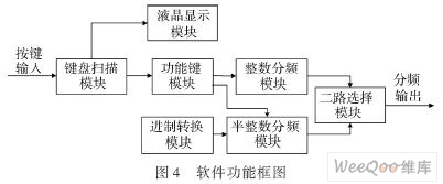
The functional block diagram of the system software is shown in Figure 4. [page]
The specific working process of the system is as follows:
The keyboard scanning module is responsible for scanning the keys, outputting the key values, and the key values are input into the 1602 LCD module for display. At the same time, the key values are input into the frequency division module in the FPGA through the function key module. When the function module is "OK", the key values are input into the FPGA frequency division module, and the frequency division coefficient N is equal to the input key value. When the function module is "cleared", the frequency division coefficient N in the FPGA frequency division module will be cleared.
3 System test and results
Test instrument: INSTEK GOS-620 (20 MHz analog oscilloscope)
Test temperature: room temperature
3.1 Check whether the system is locked
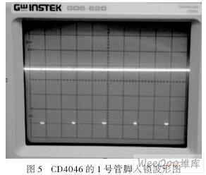
When the keyboard input is from 1 to 999.5, the waveform of the No. 1 pin of the CD4046 is shown in Figure 5, indicating that the PLL is in the locked state.
3.2 Detection of lower frequency integer/half-integer frequency division
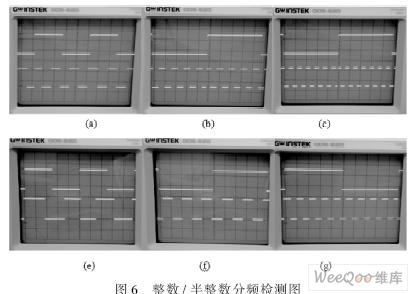
When N=3, 9, 13, 1.5, 5.5, 9.5, and the input frequency is 1 kHz, the output waveform of CD4046 is shown in Figure 6 (a), (b), (c), (e), (f), (g) respectively. It can be clearly read from the figure that the output is 3 kHz, 9 kHz, 13 kHz, 1.5 kHz, 5.5 kHz and 9.5 kHz respectively. This is consistent with the results predicted in theory.
3.3 Detection of higher frequency integer/half-integer division
When N is a higher value, it is difficult to directly see by comparing the input and output waveforms of CD4046. At this time, the input still uses a frequency value of 1kHz, and the output frequency value is directly viewed. The waveforms when N=100, 500, 999, and 999.5 are shown in Figures 7(a), (b), (c), and (d) respectively.
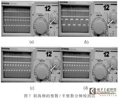
From Figure 7(a), we can see that the measured frequency is 1/(10×10-6) Hz=100 kHz.
From Figure 7(b), we can see that the measured frequency is 2/(10×10-6) Hz=500 kHz.
From Figure 7(c), we can
see that the measured frequency is approximately 1/(10×10-6) Hz=1 MHz. From Figure 7(d),
we can see that the measured value is consistent with the theoretically predicted result.
3.4 Error Analysis
The reason why the duty cycle of the waveform at a lower frequency is not the standard 50% is that the feedback signal generated after the CD4046 output frequency passes through the FPGA frequency division module is only a pulse signal. This pulse signal needs to be compared with the 1kHz standard signal entering and exiting the CD4046 for phase comparison, and the duty cycle of the standard signal is 50%. This results in the signal waveform generated after the phase comparison having a duty cycle of not 50%. The analog oscilloscope used in the system test is not very good for displaying low-frequency duty cycles other than 50%. This is most likely the main reason why the waveform is not very standard.
After the test was completed, a digital oscilloscope was used to specifically detect the output frequency of CD4046, and the result was almost consistent with the theoretical calculation.
This system combines FPGA technology, phase-locked loop technology, and frequency synthesis technology to design an integer/half-integer frequency synthesizer with an output range of 1 kHz to 999.5 kHz and a step frequency of 0.5 kHz. Compared with previous experimental devices, the system has improved performance indicators and intuitiveness. It can not only be used for teaching experiments, but also as a frequency source and frequency meter.
Keywords:FPGA PLL
Reference address:Design of PLL Frequency Synthesizer Based on FPGA
1 Basic principles of PLL frequency synthesizer
Frequency synthesizers are mainly divided into four types: direct, phase-locked, direct digital, and hybrid. At present, phase-locked and digital types are easy to realize serialization, miniaturization, modularization, and engineering, and their performance is getting better and better. They have gradually become the most typical and widely used frequency synthesizers [1]. This paper mainly adopts the integrated phase-locked loop PLL phase-Lockde Loop chip CD4046 and uses FPGA to realize PLL frequency synthesizer.
Phase-locked frequency synthesizer is composed of PLL. The principle block diagram of a typical phase-locked frequency synthesizer is shown in Figure 1.

Its working process can be simply described as follows: the average DC value of the phase detector output current multiplied by the impedance of the loop filter forms the input control voltage of the VCO. The VCO is a voltage-frequency conversion device with a proportional constant. The control voltage of the loop filter adjusts the output phase of the VCO, and after dividing by N, it is equal to the phase of the comparison frequency. Because the phase is the integral of the frequency, this process also applies to the frequency. The output frequency can be expressed as:

Formula 1 is only valid when the PLL is in the locked state, and it is not valid in the intermediate process of the PLL being readjusted to the locked state. In actual applications, the R value is fixed, the N value is variable [2], and XTAL is the frequency of the input signal.
2 System Design
The functions of the entire system are mainly implemented by the FPGA chip EPF10K10 LC84-4 to control related hardware. The principle block diagram of this system is shown in Figure 2.

As can be seen from Figure 2, on the one hand, the 40 MHz active crystal oscillator is divided by the control of the FPGA to obtain a 1 kHz frequency signal, which is used as the input reference frequency division of the CD4046. The output signal of the VCO of the CD4046 is directly input into the integer frequency division module and the half-integer frequency division module; on the other hand, the keyboard scans and outputs the key value, which is sent to the functional module. If the functional module indicates "OK", the key value is sent as the frequency division coefficient to the integer frequency division module and the half-integer frequency division module to divide the signal input by the VCO respectively; if the functional module indicates "clear", the frequency division coefficient is cleared. The last bit of the key value directly controls the two-way selection module: if the last bit of the key value is "0", the two-way selection module is controlled to output the integer module result; if the last bit of the key value is "5", the two-way selection module is controlled to output the half-integer module result. The result of the frequency division output is compared with the reference frequency of the phase-locked loop in the phase detector, and a Ud voltage signal corresponding to the phase difference of the two signals is generated. The high-frequency components and noise in Ud are filtered out by the loop filter, and Uc is output. Uc is then input into the VCO, so that the oscillation frequency of the voltage-controlled oscillator keeps approaching the frequency of the input signal, and finally the loop is locked, and the VCO outputs a stable frequency.
During the operation, the FPGA controls the change of the preset N/N+0.5. When N/N+0.5 changes, the output signal frequency response changes with the input signal. At the same time, the FPGA also realizes the functions of keyboard scanning and LCD display.
2.1 System hardware design
The hardware is shown in Figure 3. The system part is mainly composed of 7 parts: external system clock, 4×4 keyboard control circuit, FPGA processing chip, EPC2LC20 EPROM chip, PLL chip CD4046 and its peripheral circuit, LCD 1602 display module, oscilloscope. This design uses the FPGA dedicated configuration chip EPC2, and downloads the program to the FPGA chip multiple times through the download cable ByteBlaster MV. The system uses FPGA chip as the control center, inputs control information by key scanning, and displays it on the LCD screen. It can conveniently and intuitively demonstrate the application of PLL chip CD4046 in frequency synthesis technology, and achieve the expected index requirements. The specific models of the main hardware in this design are: LCD TC1602A-01T, FPGA chip EPF10K10LC84-4, 40.000 MHz active crystal oscillator HO-12B.

2.2 System software design
By writing VHDL program to realize integer/half-integer frequency division, and using Quartus II and ModelSim, the author completed the design and simulation of VHDL program.
The functional block diagram of the system software is shown in Figure 4. [page]

The specific working process of the system is as follows:
The keyboard scanning module is responsible for scanning the keys, outputting the key values, and the key values are input into the 1602 LCD module for display. At the same time, the key values are input into the frequency division module in the FPGA through the function key module. When the function module is "OK", the key values are input into the FPGA frequency division module, and the frequency division coefficient N is equal to the input key value. When the function module is "cleared", the frequency division coefficient N in the FPGA frequency division module will be cleared.
3 System test and results
Test instrument: INSTEK GOS-620 (20 MHz analog oscilloscope)
Test temperature: room temperature
3.1 Check whether the system is locked
When the keyboard input is from 1 to 999.5, the waveform of the No. 1 pin of the CD4046 is shown in Figure 5, indicating that the PLL is in the locked state.

3.2 Detection of lower frequency integer/half-integer frequency division
When N=3, 9, 13, 1.5, 5.5, 9.5, and the input frequency is 1 kHz, the output waveform of CD4046 is shown in Figure 6 (a), (b), (c), (e), (f), (g) respectively. It can be clearly read from the figure that the output is 3 kHz, 9 kHz, 13 kHz, 1.5 kHz, 5.5 kHz and 9.5 kHz respectively. This is consistent with the results predicted in theory.

3.3 Detection of higher frequency integer/half-integer division
When N is a higher value, it is difficult to directly see by comparing the input and output waveforms of CD4046. At this time, the input still uses a frequency value of 1kHz, and the output frequency value is directly viewed. The waveforms when N=100, 500, 999, and 999.5 are shown in Figures 7(a), (b), (c), and (d) respectively.

From Figure 7(a), we can see that the measured frequency is 1/(10×10-6) Hz=100 kHz.
From Figure 7(b), we can see that the measured frequency is 2/(10×10-6) Hz=500 kHz.
From Figure 7(c), we can
see that the measured frequency is approximately 1/(10×10-6) Hz=1 MHz. From Figure 7(d),
we can see that the measured value is consistent with the theoretically predicted result.
3.4 Error Analysis
The reason why the duty cycle of the waveform at a lower frequency is not the standard 50% is that the feedback signal generated after the CD4046 output frequency passes through the FPGA frequency division module is only a pulse signal. This pulse signal needs to be compared with the 1kHz standard signal entering and exiting the CD4046 for phase comparison, and the duty cycle of the standard signal is 50%. This results in the signal waveform generated after the phase comparison having a duty cycle of not 50%. The analog oscilloscope used in the system test is not very good for displaying low-frequency duty cycles other than 50%. This is most likely the main reason why the waveform is not very standard.
After the test was completed, a digital oscilloscope was used to specifically detect the output frequency of CD4046, and the result was almost consistent with the theoretical calculation.
This system combines FPGA technology, phase-locked loop technology, and frequency synthesis technology to design an integer/half-integer frequency synthesizer with an output range of 1 kHz to 999.5 kHz and a step frequency of 0.5 kHz. Compared with previous experimental devices, the system has improved performance indicators and intuitiveness. It can not only be used for teaching experiments, but also as a frequency source and frequency meter.
Previous article:Design of a high-precision frequency meter with wide input range
Next article:Research on Testing Technology of 16-bit Microprocessor L80C186-10
Recommended ReadingLatest update time:2024-11-16 21:59
Design and verification of DDR read and write control using FPGA IP
Introduction With the continuous development of high-speed processors, the application fields of embedded systems are becoming more and more extensive, the scale of digital signal processing is also getting larger and larger, and the size of RAM in the system is increasing, such as video surveillance, image data acqu
[Embedded]
Developing video algorithms using FPGAs for image and real-time video processing

The human brain is the most advanced compact processing unit we know of; however, improvements in image processing may soon allow machines to surpass us, thanks to new processors, tools, architectures, and software. New technologies and the rapid pace of their adoption offer huge potential for industrial manufacturi
[Embedded]

Design of a universal flight control computer platform based on FPGA+DSP

The flight control computer is the core device of modern missile guidance and control system. Its performance is directly related to the accuracy of precision guidance and the probability of killing the target. In recent years, missile-borne equipment such as servos, seekers, and inertial navigation have been increa
[Embedded]

300MSPS high speed 10-bit D/A converter AD9751
Abstract: AD9751 is a high-speed digital-to-analog converter with a conversion rate up to 300MSPS. It has many advantages such as dual-port input, high conversion accuracy, fast speed, low power consumption, and low cost. It has excellent AC and DC characteristics at the same time and can be widely used in applic
[Analog Electronics]
An FPGA Design and Application of Taxi Meter

O Introduction
FPGA (Field Programmable Gate Array) is a high-density programmable logic device that supports system programming and can implement different logic functions by writing different configuration data. Using FPGA to design electronic systems has obvious characteristics such as short design cycle
[Embedded]

Design of Programmable PWM Circuit Based on FPGA
The H-bridge drive
circuit
in a certain system
needs to use two pulse width modulator (PWM) signals to
drive
a motor to
control
its forward and reverse directions, and the two signals must have a certain time interval to avoid excessive drive current and damage to the drive components. I
[Analog Electronics]
Design of D/A Converter Circuit Based on AD7543 and FPGA
introduction
The digital/analog conversion (D/A) circuit is one of the commonly used circuits in digital systems. Its main function is to convert digital signals into analog signals, which is usually achieved using a dedicated digital/analog conversion (D/A) chip. AD7543 is a 12-bit digital/analog conve
[Analog Electronics]
Design of Programmable Filter Measurement System Based on FPGA and Quartus II

1. Introduction Amplifiers and filters are important components of modern electronic systems, and the quality of their performance indicators directly determines the performance of the entire system. Most traditional amplifiers and filters have fixed amplification factors and fixed cutoff frequencies. In many engineer
[Power Management]

- Popular Resources
- Popular amplifiers
-
 Analysis and Implementation of MAC Protocol for Wireless Sensor Networks (by Yang Zhijun, Xie Xianjie, and Ding Hongwei)
 -
 MATLAB and FPGA implementation of wireless communication
 -
 Intelligent computing systems (Chen Yunji, Li Ling, Li Wei, Guo Qi, Du Zidong)
 -
 Summary of non-synthesizable statements in FPGA
Recommended Content
Latest Test Measurement Articles
- Keysight Technologies Helps Samsung Electronics Successfully Validate FiRa® 2.0 Safe Distance Measurement Test Case
- From probes to power supplies, Tektronix is leading the way in comprehensive innovation in power electronics testing
- Seizing the Opportunities in the Chinese Application Market: NI's Challenges and Answers
- Tektronix Launches Breakthrough Power Measurement Tools to Accelerate Innovation as Global Electrification Accelerates
- Not all oscilloscopes are created equal: Why ADCs and low noise floor matter
- Enable TekHSI high-speed interface function to accelerate the remote transmission of waveform data
- How to measure the quality of soft start thyristor
- How to use a multimeter to judge whether a soft starter is good or bad
- What are the advantages and disadvantages of non-contact temperature sensors?
MoreSelected Circuit Diagrams
MorePopular Articles
- Innolux's intelligent steer-by-wire solution makes cars smarter and safer
- 8051 MCU - Parity Check
- How to efficiently balance the sensitivity of tactile sensing interfaces
- What should I do if the servo motor shakes? What causes the servo motor to shake quickly?
- 【Brushless Motor】Analysis of three-phase BLDC motor and sharing of two popular development boards
- Midea Industrial Technology's subsidiaries Clou Electronics and Hekang New Energy jointly appeared at the Munich Battery Energy Storage Exhibition and Solar Energy Exhibition
- Guoxin Sichen | Application of ferroelectric memory PB85RS2MC in power battery management, with a capacity of 2M
- Analysis of common faults of frequency converter
- In a head-on competition with Qualcomm, what kind of cockpit products has Intel come up with?
- Dalian Rongke's all-vanadium liquid flow battery energy storage equipment industrialization project has entered the sprint stage before production
MoreDaily News
- Allegro MicroSystems Introduces Advanced Magnetic and Inductive Position Sensing Solutions at Electronica 2024
- Car key in the left hand, liveness detection radar in the right hand, UWB is imperative for cars!
- After a decade of rapid development, domestic CIS has entered the market
- Aegis Dagger Battery + Thor EM-i Super Hybrid, Geely New Energy has thrown out two "king bombs"
- A brief discussion on functional safety - fault, error, and failure
- In the smart car 2.0 cycle, these core industry chains are facing major opportunities!
- The United States and Japan are developing new batteries. CATL faces challenges? How should China's new energy battery industry respond?
- Murata launches high-precision 6-axis inertial sensor for automobiles
- Ford patents pre-charge alarm to help save costs and respond to emergencies
- New real-time microcontroller system from Texas Instruments enables smarter processing in automotive and industrial applications
Guess you like
- SHT31 Review + Unboxing Test
- How to obtain high-frequency equivalent models of devices such as varistors and TVS transient diodes
- MicroPython uses the new neopixel driver
- Review Weekly Report 20220509: Saifang RISC-V Linux Starlight Board is coming, how is the Xianji 800MHz HPM6750 tested?
- How to set default rules for Altium drawing?
- Matlab and Modelsim co-simulation error
- ST NUCLEO-G071RB evaluation application - Come and experience the new generation of entry-level 32-bit STM32, giving you the best cost-effective experience
- Security innovation, a new verification method. Download Fujitsu's "Spectrum Verification Solution" white paper and get a gift!
- Which forum member has a deeper understanding of MOS tubes? I usually overlook some parameters when reading the specification, and I want to understand them all today. Know...
- How to configure the SSH service of Win10 Linux subsystem

 Analysis and Implementation of MAC Protocol for Wireless Sensor Networks (by Yang Zhijun, Xie Xianjie, and Ding Hongwei)


 京公网安备 11010802033920号