Circular Logic
"Is this a riddle?" you ask. Of course not. The title sounds like a loop, real circular logic, but it illustrates a point. Typical (typ) is often the most misunderstood word in integrated circuit (IC) testing, and other words can be used to describe the concept: representative, indicative, general, normal, standard, mainstream, average, medium, customary. Confused? In the IC world, typical is usually defined as a characteristic of a group of devices. OK, but that's really "beating around the bush," as the old saying goes. Let me tell you a little IC testing trick. "Typical" in an IC data sheet means untested. The secret is out! So why do IC manufacturers go to the trouble of giving typical values? Let me explain.
Typical Values vs. Variations
IC typical values are statistical values, so they cannot be directly tested. For example, it's like saying that the average height of an adult human is 5 feet 5 inches. Measuring any single person does not determine the medium, average, or typical height. Anthropologists can measure the height of each ethnic group or measure a sample of the population statistically, and then statisticians can calculate the confidence level of the average given the sample size. The same statistical process is used for ICs. IC designers can statistically predict typical values based on simulation test results. Again, typical values are averaged to provide general guidance to circuit designers.
Specifications listed in IC data sheets are usually of the following types:
● Absolute maximum values mean that these values must not be exceeded or the device may be damaged.
● Electrical characteristics are general test conditions unless otherwise noted.
● Minimum (min), typical (typ), and maximum (max) specifications are measured values under specified units and conditions. Note that "conditions" are in addition to "unless otherwise specified."
● Notes change, limit, and declare the items tested and the test methods.
To help understand, let's take a common example. The following is a general rule in various data sheets from different IC manufacturers.
Unless otherwise stated, the minimum and maximum values are tested as specified in the general conditions of electrical characteristics. The expression may be: "TA = TMIN to TMAX, unless otherwise stated. Typical values are values at TA = +25°C." This means that the ambient temperature (TA) is equal to the minimum and maximum temperatures listed for the operating temperature, unless otherwise stated by the manufacturer. Typical values are values only at TA = +25°C. Then there are notes, the most common of which are:
Note 1: All devices are 100% production tested at +25°C. The conditions listed for TA = TMIN to TMAX are guaranteed by design.
Note 2: Linearity tested within GND + 20mV and AVDD - 20mV. Gain and offset errors are allowed.
Note 3: Codes above 2047 are guaranteed to be within ±8 LSB (least significant bit).
Note 4: Gain and offset tested within GND + 100mV and AVDD - 100mV.
Note 5: Guaranteed by design
. The words "guaranteed by design" are at the end of Notes 1 and 5. This sentence is very meaningful. All IC manufacturing (fab) processes have variations. Because the components and multiple layers are very small, almost anything can cause variations. These deviations are part of the normal range of variation.
We will borrow part of the MAX5134 to MAX5137 data sheet (Figure 1) to explain these notes.
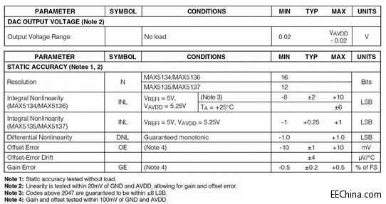
Figure 1. Excerpt from the MAX5134 to Max5137 digital-to-analog converter (DAC) family data sheet.
Note 1 means that statistical accuracy is tested only at room temperature (+25°C), regardless of the temperature stated earlier in the data sheet. Other operating temperature ranges are covered by "guaranteed by design." (We'll get to that shortly.)
Notes 2 and 4 are common to rail-to-rail op amps and buffered-output DACs. Note that the output voltage range is calculated with "no load." This is because rail-to-rail operation is, frankly, wishful thinking. It's not perfect, but it's much better than earlier devices whose output circuits deviated from the supply voltage when sourcing current.
Note 3 is common to DACs. Codes below some number near the bottom (usually ground) and above some number near the top rail are less linear than the middle codes. Here, with a total of 65,536 codes, the INL (integral nonlinearity) for the bottom code, 2047, is ±10 LSB; above 2047, the INL is only ±8 LSB.
Let me digress. Imagine buying paint for your home. The home furnishing store advises you to pick a color cloth so that it can be accurately matched on their color matching machine. Then they apply a white primer and the color matching machine automatically adds multiple pigments to get an "exact match." This process is repeated for each can of paint purchased. Once all the paints are accurately matched, what do they tell you to do? What would a professional painter do? Mix the paint from all the cans together. Why? The human eye and brain can distinguish colors more accurately, so they can see color errors between different mixed paints on the "exact match" machine. It's not all the machine's fault. The mixer's metering valves, color separation filters, gain and offset calibrations are not perfect. Even the pigments themselves have an acceptable range of colors and viscosities. As the spraying process continues, various tolerances are added, combined, and sometimes even multiplied, resulting in small but visible errors - the range of variation, the standard deviation.
Figure 2 shows a common acceptable standard deviation or bell curve. The solid black line shows a normal distribution, which is what we want. The dashed green line shows that the process is moving to the right of center - hopefully we understand the cause of the deviation so we can correct it. The blue dashed line is a bifurcated curve, where two parameters may vary. When many different factors vary, more complex curves are formed. This is why professional painters mix all the paint in the cans before painting the wall. Isn't the average error amazing? [page]
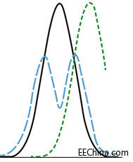
Figure 2. Process standard deviation or bell curve. The more factors that vary, the more complex the curve.
Compensating for process variation
To ensure that the IC meets its specifications, multiple layers of engineering safeguards are designed into the IC manufacturing process to average out possible errors. No engineering group wants to ship a device that is “out of specification.” So, designers leave plenty of wiggle room in device specifications, while test and QA engineers want to expect variations to meet “six-sigma specification limits.” The resulting performance specifications are very conservative. The
design process compensates for many design, manufacturing, and process differences. So designers use simulation tools to study the variations in the manufacturing process, “process corners.” The reasoning is simple. If they are worried about process corners, the process is well centered. Then they modify the circuit to be as immune to these process corners as possible. The most extreme process corners are fast hot and slow cold (see Figure 3). Hot and cold refer to temperature. Fast means high gain, high electron mobility; slow means the opposite. Designers can optimize design criteria, but they cannot optimize all factors. So, unspecified parameters are not addressed.
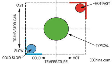
Figure 3. IC manufacturing process variation.
Understanding 6σ2
The concept of 6σ was first proposed by Bill Smith of Motorola in 1986 as a set of standards designed to improve manufacturing processes and avoid defects. Sigma (lowercase Greek letter σ) is used to represent the standard deviation of a statistical population (i.e., the parameter that represents variation). The term "6σ process" means that if there are 6 standard deviations between the process mean and the nearest specification limit, then the specification requirements are almost perfectly met. This conclusion is based on the calculation method used in process capability analysis.
In capability analysis, the number of standard deviations between the process mean and the nearest specification limit is given in σ units. As the process standard deviation increases, or the process mean moves away from the center of the tolerance, the number of standard deviations between the mean and the nearest specification limit will decrease, which reduces the σ number.
The role of 1.5σ shift
Experience shows that the long-term performance of a process is often inferior to the short-term performance. Therefore, the σ number between the process mean and the nearest specification limit is likely to decrease over time. This is proven to be the case by the initial short-term analysis. To account for the actual increase in process shifts over time, an empirically based 1.5σ shift is introduced into the calculations. Based on this premise, a process that has 6σ between the process mean and the nearest specification limit in the short-term analysis will have 4.5σ in the long-term. This can happen because the process mean will shift over time, or the long-term standard deviation of the process will be larger than the standard deviation observed in the short-term, or both.
Therefore, the widely accepted definition of a 6σ process is 3.4 defects per million opportunities (DPMO). This definition is based on the fact that for a normally distributed process, the number of points that are 4.5 standard deviations above or below the mean is 3.4 parts per million. (This is a one-sided capability analysis). Therefore, a 3.4 DPMO for 6σ actually corresponds to 4.5σ, which is nominally 6σ, minus the 1.5σ shift to account for long-term variation. This theory is designed to prevent underestimation of defect rates, which is likely to occur in practice.
When considering a 1.5σ shift, the short-term σ levels correspond to the following long-term DPMO values (one-sided).
●1 σ = 690,000 DPMO = 31% efficiency
●2 σ = 308,000 DPMO = 69.2% efficiency
●3 σ = 66,800 DPMO = 93.32% efficiency
●4 σ = 6,210 DPMO = 99.379% efficiency
●5 σ = 230 DPMO = 99.977% efficiency
●6 σ = 3.4 DPMO = 99.9997% efficiencyConclusion
I
believe the above discussion helps explain the reasoning behind wafer testing and how typical (i.e., how normal) typical values are.
Now, let's take it a step further. Suppose we are designing a measurement instrument for use in a test lab environment. To set the instrument specifications, we need to understand and control component manufacturing variations. Knowing that the accuracy of the IC used is 6σ will help increase our confidence in the final instrument specifications. Here, we limit the instrument to operating in room temperature. You may have overlooked it, but we specified "test lab environment" above. This is a critical specification. If the instrument is to be used in the field, the temperature, humidity, and atmospheric pressure of the specific work site must be clearly defined. For medical use, we must specify which parts are related to the patient, such as those that need to be sterilized or disposable. If the instrument can be used in space or on a rocket, what kind of vibration, atmospheric pressure, radiation resistance, and temperature resistance are required?
Reference address:"Typical values" are usually tested in a typical manner
"Is this a riddle?" you ask. Of course not. The title sounds like a loop, real circular logic, but it illustrates a point. Typical (typ) is often the most misunderstood word in integrated circuit (IC) testing, and other words can be used to describe the concept: representative, indicative, general, normal, standard, mainstream, average, medium, customary. Confused? In the IC world, typical is usually defined as a characteristic of a group of devices. OK, but that's really "beating around the bush," as the old saying goes. Let me tell you a little IC testing trick. "Typical" in an IC data sheet means untested. The secret is out! So why do IC manufacturers go to the trouble of giving typical values? Let me explain.
Typical Values vs. Variations
IC typical values are statistical values, so they cannot be directly tested. For example, it's like saying that the average height of an adult human is 5 feet 5 inches. Measuring any single person does not determine the medium, average, or typical height. Anthropologists can measure the height of each ethnic group or measure a sample of the population statistically, and then statisticians can calculate the confidence level of the average given the sample size. The same statistical process is used for ICs. IC designers can statistically predict typical values based on simulation test results. Again, typical values are averaged to provide general guidance to circuit designers.
Specifications listed in IC data sheets are usually of the following types:
● Absolute maximum values mean that these values must not be exceeded or the device may be damaged.
● Electrical characteristics are general test conditions unless otherwise noted.
● Minimum (min), typical (typ), and maximum (max) specifications are measured values under specified units and conditions. Note that "conditions" are in addition to "unless otherwise specified."
● Notes change, limit, and declare the items tested and the test methods.
To help understand, let's take a common example. The following is a general rule in various data sheets from different IC manufacturers.
Unless otherwise stated, the minimum and maximum values are tested as specified in the general conditions of electrical characteristics. The expression may be: "TA = TMIN to TMAX, unless otherwise stated. Typical values are values at TA = +25°C." This means that the ambient temperature (TA) is equal to the minimum and maximum temperatures listed for the operating temperature, unless otherwise stated by the manufacturer. Typical values are values only at TA = +25°C. Then there are notes, the most common of which are:
Note 1: All devices are 100% production tested at +25°C. The conditions listed for TA = TMIN to TMAX are guaranteed by design.
Note 2: Linearity tested within GND + 20mV and AVDD - 20mV. Gain and offset errors are allowed.
Note 3: Codes above 2047 are guaranteed to be within ±8 LSB (least significant bit).
Note 4: Gain and offset tested within GND + 100mV and AVDD - 100mV.
Note 5: Guaranteed by design
. The words "guaranteed by design" are at the end of Notes 1 and 5. This sentence is very meaningful. All IC manufacturing (fab) processes have variations. Because the components and multiple layers are very small, almost anything can cause variations. These deviations are part of the normal range of variation.
We will borrow part of the MAX5134 to MAX5137 data sheet (Figure 1) to explain these notes.

Figure 1. Excerpt from the MAX5134 to Max5137 digital-to-analog converter (DAC) family data sheet.
Note 1 means that statistical accuracy is tested only at room temperature (+25°C), regardless of the temperature stated earlier in the data sheet. Other operating temperature ranges are covered by "guaranteed by design." (We'll get to that shortly.)
Notes 2 and 4 are common to rail-to-rail op amps and buffered-output DACs. Note that the output voltage range is calculated with "no load." This is because rail-to-rail operation is, frankly, wishful thinking. It's not perfect, but it's much better than earlier devices whose output circuits deviated from the supply voltage when sourcing current.
Note 3 is common to DACs. Codes below some number near the bottom (usually ground) and above some number near the top rail are less linear than the middle codes. Here, with a total of 65,536 codes, the INL (integral nonlinearity) for the bottom code, 2047, is ±10 LSB; above 2047, the INL is only ±8 LSB.
Let me digress. Imagine buying paint for your home. The home furnishing store advises you to pick a color cloth so that it can be accurately matched on their color matching machine. Then they apply a white primer and the color matching machine automatically adds multiple pigments to get an "exact match." This process is repeated for each can of paint purchased. Once all the paints are accurately matched, what do they tell you to do? What would a professional painter do? Mix the paint from all the cans together. Why? The human eye and brain can distinguish colors more accurately, so they can see color errors between different mixed paints on the "exact match" machine. It's not all the machine's fault. The mixer's metering valves, color separation filters, gain and offset calibrations are not perfect. Even the pigments themselves have an acceptable range of colors and viscosities. As the spraying process continues, various tolerances are added, combined, and sometimes even multiplied, resulting in small but visible errors - the range of variation, the standard deviation.
Figure 2 shows a common acceptable standard deviation or bell curve. The solid black line shows a normal distribution, which is what we want. The dashed green line shows that the process is moving to the right of center - hopefully we understand the cause of the deviation so we can correct it. The blue dashed line is a bifurcated curve, where two parameters may vary. When many different factors vary, more complex curves are formed. This is why professional painters mix all the paint in the cans before painting the wall. Isn't the average error amazing? [page]

Figure 2. Process standard deviation or bell curve. The more factors that vary, the more complex the curve.
Compensating for process variation
To ensure that the IC meets its specifications, multiple layers of engineering safeguards are designed into the IC manufacturing process to average out possible errors. No engineering group wants to ship a device that is “out of specification.” So, designers leave plenty of wiggle room in device specifications, while test and QA engineers want to expect variations to meet “six-sigma specification limits.” The resulting performance specifications are very conservative. The
design process compensates for many design, manufacturing, and process differences. So designers use simulation tools to study the variations in the manufacturing process, “process corners.” The reasoning is simple. If they are worried about process corners, the process is well centered. Then they modify the circuit to be as immune to these process corners as possible. The most extreme process corners are fast hot and slow cold (see Figure 3). Hot and cold refer to temperature. Fast means high gain, high electron mobility; slow means the opposite. Designers can optimize design criteria, but they cannot optimize all factors. So, unspecified parameters are not addressed.

Figure 3. IC manufacturing process variation.
Understanding 6σ2
The concept of 6σ was first proposed by Bill Smith of Motorola in 1986 as a set of standards designed to improve manufacturing processes and avoid defects. Sigma (lowercase Greek letter σ) is used to represent the standard deviation of a statistical population (i.e., the parameter that represents variation). The term "6σ process" means that if there are 6 standard deviations between the process mean and the nearest specification limit, then the specification requirements are almost perfectly met. This conclusion is based on the calculation method used in process capability analysis.
In capability analysis, the number of standard deviations between the process mean and the nearest specification limit is given in σ units. As the process standard deviation increases, or the process mean moves away from the center of the tolerance, the number of standard deviations between the mean and the nearest specification limit will decrease, which reduces the σ number.
The role of 1.5σ shift
Experience shows that the long-term performance of a process is often inferior to the short-term performance. Therefore, the σ number between the process mean and the nearest specification limit is likely to decrease over time. This is proven to be the case by the initial short-term analysis. To account for the actual increase in process shifts over time, an empirically based 1.5σ shift is introduced into the calculations. Based on this premise, a process that has 6σ between the process mean and the nearest specification limit in the short-term analysis will have 4.5σ in the long-term. This can happen because the process mean will shift over time, or the long-term standard deviation of the process will be larger than the standard deviation observed in the short-term, or both.
Therefore, the widely accepted definition of a 6σ process is 3.4 defects per million opportunities (DPMO). This definition is based on the fact that for a normally distributed process, the number of points that are 4.5 standard deviations above or below the mean is 3.4 parts per million. (This is a one-sided capability analysis). Therefore, a 3.4 DPMO for 6σ actually corresponds to 4.5σ, which is nominally 6σ, minus the 1.5σ shift to account for long-term variation. This theory is designed to prevent underestimation of defect rates, which is likely to occur in practice.
When considering a 1.5σ shift, the short-term σ levels correspond to the following long-term DPMO values (one-sided).
●1 σ = 690,000 DPMO = 31% efficiency
●2 σ = 308,000 DPMO = 69.2% efficiency
●3 σ = 66,800 DPMO = 93.32% efficiency
●4 σ = 6,210 DPMO = 99.379% efficiency
●5 σ = 230 DPMO = 99.977% efficiency
●6 σ = 3.4 DPMO = 99.9997% efficiencyConclusion
I
believe the above discussion helps explain the reasoning behind wafer testing and how typical (i.e., how normal) typical values are.
Now, let's take it a step further. Suppose we are designing a measurement instrument for use in a test lab environment. To set the instrument specifications, we need to understand and control component manufacturing variations. Knowing that the accuracy of the IC used is 6σ will help increase our confidence in the final instrument specifications. Here, we limit the instrument to operating in room temperature. You may have overlooked it, but we specified "test lab environment" above. This is a critical specification. If the instrument is to be used in the field, the temperature, humidity, and atmospheric pressure of the specific work site must be clearly defined. For medical use, we must specify which parts are related to the patient, such as those that need to be sterilized or disposable. If the instrument can be used in space or on a rocket, what kind of vibration, atmospheric pressure, radiation resistance, and temperature resistance are required?
Previous article:AMETEK Aerospace Standard Test Solutions
Next article:Providing test systems for car radio and GPS
Recommended Content
Latest Test Measurement Articles
- Keysight Technologies Helps Samsung Electronics Successfully Validate FiRa® 2.0 Safe Distance Measurement Test Case
- From probes to power supplies, Tektronix is leading the way in comprehensive innovation in power electronics testing
- Seizing the Opportunities in the Chinese Application Market: NI's Challenges and Answers
- Tektronix Launches Breakthrough Power Measurement Tools to Accelerate Innovation as Global Electrification Accelerates
- Not all oscilloscopes are created equal: Why ADCs and low noise floor matter
- Enable TekHSI high-speed interface function to accelerate the remote transmission of waveform data
- How to measure the quality of soft start thyristor
- How to use a multimeter to judge whether a soft starter is good or bad
- What are the advantages and disadvantages of non-contact temperature sensors?
MoreSelected Circuit Diagrams
MorePopular Articles
- Innolux's intelligent steer-by-wire solution makes cars smarter and safer
- 8051 MCU - Parity Check
- How to efficiently balance the sensitivity of tactile sensing interfaces
- What should I do if the servo motor shakes? What causes the servo motor to shake quickly?
- 【Brushless Motor】Analysis of three-phase BLDC motor and sharing of two popular development boards
- Midea Industrial Technology's subsidiaries Clou Electronics and Hekang New Energy jointly appeared at the Munich Battery Energy Storage Exhibition and Solar Energy Exhibition
- Guoxin Sichen | Application of ferroelectric memory PB85RS2MC in power battery management, with a capacity of 2M
- Analysis of common faults of frequency converter
- In a head-on competition with Qualcomm, what kind of cockpit products has Intel come up with?
- Dalian Rongke's all-vanadium liquid flow battery energy storage equipment industrialization project has entered the sprint stage before production
MoreDaily News
- Allegro MicroSystems Introduces Advanced Magnetic and Inductive Position Sensing Solutions at Electronica 2024
- Car key in the left hand, liveness detection radar in the right hand, UWB is imperative for cars!
- After a decade of rapid development, domestic CIS has entered the market
- Aegis Dagger Battery + Thor EM-i Super Hybrid, Geely New Energy has thrown out two "king bombs"
- A brief discussion on functional safety - fault, error, and failure
- In the smart car 2.0 cycle, these core industry chains are facing major opportunities!
- The United States and Japan are developing new batteries. CATL faces challenges? How should China's new energy battery industry respond?
- Murata launches high-precision 6-axis inertial sensor for automobiles
- Ford patents pre-charge alarm to help save costs and respond to emergencies
- New real-time microcontroller system from Texas Instruments enables smarter processing in automotive and industrial applications
Guess you like
- What is ISO 17025 and why is it important?
- Practice together in 2021 + review the gains and losses of 2020 work
- What to do if SYSTEM is not found in the AD status bar?
- Single analog signal input channel detects multiple signal major problems
- FPGA Design Tips
- Easy to understand and not esoteric: "Power Supply Design" - Fundamentals of Electronic Design
- EEWORLD University Hall ---- Electromagnetic Field and Electromagnetic Wave
- About the development of ST's 8032 core microcontroller uPSD3234A-40u
- I burned a stmf103 minimum board today
- Basic knowledge of embedded Linux development

 A Practical Tutorial on ASIC Design (Compiled by Yu Xiqing)


 京公网安备 11010802033920号