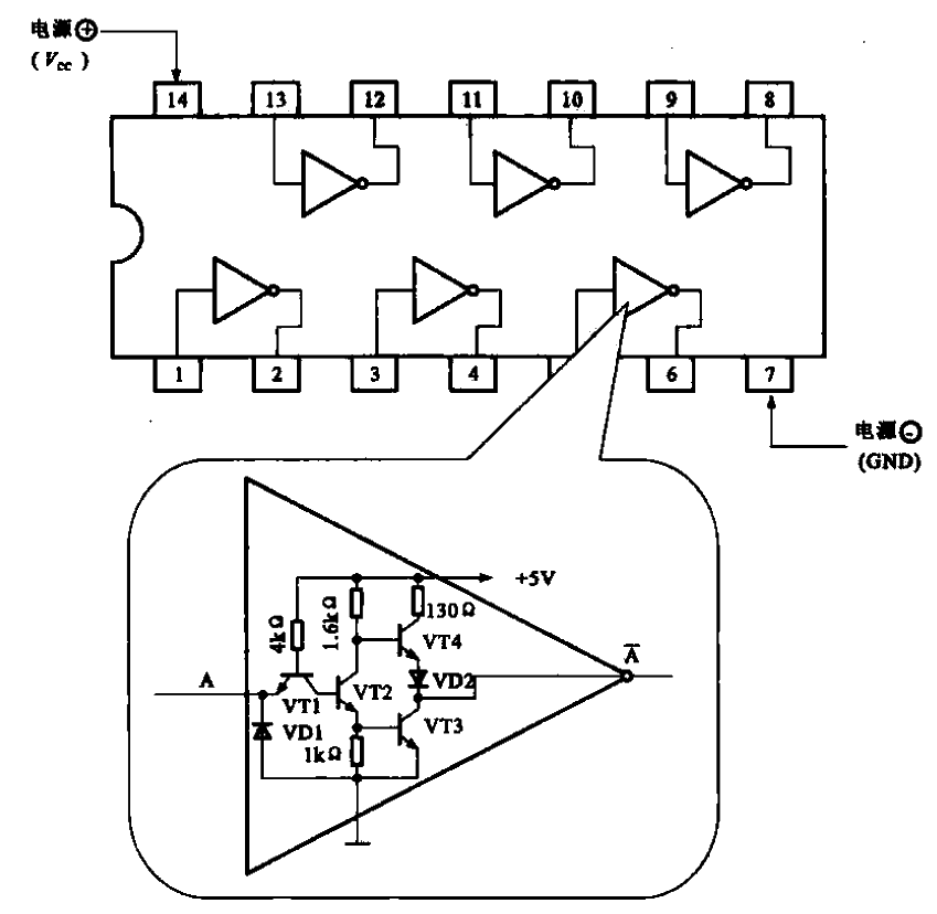
TTL inverter circuit and its internal structure
Source: InternetPublisher:ghaytweyhtoo Keywords: TTL BSP Updated: 2021/05/14

Shown is a TTL integrated circuit with 6 inverters (SN7404, M53204P). The internal circuit structure of each inverter
is also shown in the figure.
The DC voltage +5 V provides power for each inverter. When the input terminal A is high level (number "l"), the transistor VT1 is turned off,
the transistor VT2 is turned on, the diode VD2 is turned off, the transistor VT3 is turned on, and the output terminal A is low level (digit "o"). If the input terminal
A is low level (digital "O"), the circuit undergoes a reverse phase change, then the output terminal A is high level ,
- What is the difference between CPLD and FPGA?
- DIY a decorative lamp
- Basic characteristics/working principles and application circuits of tunnel diodes
- Share an interesting LED decoration project
- Make a flameless electronic candle using simple electronics and LEDs
- What types of force sensors are there?
- Make a simple AM radio with digital circuit
- An easy-to-make counting frequency meter
- Symmetrical output three-way frequency circuit (74LS109, 74LS113)
- Environmentally friendly and energy-saving LED AC/DC dual-purpose lamp
- Poultry warming temperature control circuit
- Proportional frequency discriminator circuit
- Double detuned loop frequency discriminator circuit
- collector amplitude modulation circuit
- Schiller oscillator circuit
- Differential Amplifier Circuit
- color discrimination circuit
- Guest arrival signal recognition circuit
- Fault signal trip circuit
- Small current generator circuit


 京公网安备 11010802033920号