What is the difference between CPLD and FPGA?
Source: InternetPublisher:李商隐身 Keywords: fpga cpld programmable logic Updated: 2025/01/14
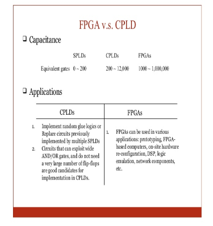
Programmable logic includes PAL, GAL, PLD, etc. Through continuous development, it has developed into the current CPLD/FPGA. The functions of CPLD (Complex Programmable Logic Device) and FPGA (Field Programmable Gate Array) are basically the same, but the implementation principles are slightly different. When ignoring the differences between the two, they can be called programmable logic devices or CPLD/FPGA. The implementation of CPLD is based on the product terminology structure. FPGA is based on the lookup table structure.

CPLD and FPGA
The difference between the two is usually characterized by:
1.CPLD has large logic cells, small capacity, deterministic timing, and can predict delays based on a lookup table (LUT-based), so the timing depends on the routing of the lookup table.
2.CPLD generally has a smaller capacity and fewer registers, so it is suitable for designing some small-capacity complex combinational logic, such as address decoders, bus interfaces, and power-on reset logic. On the other hand, FPGA can do some large-capacity advanced designs, such as embedded CPUs, data processing, etc.
3. The internal connection of CPLD adopts continuous internal connection, so the link delay is fixed, but affected by the connection path, FPGA uses segmented links to make full use of connection resources.
4.FPGA can provide sufficient logic capacity density than CPLD devices, greatly reducing PCB space and reducing system power consumption.
The differences between CPLD and FPGA are as described above, but as programmable logic devices, they have common characteristics and can generally be composed of three parts:
1. A two-dimensional array of logic (logic cells) that forms the core of a device's logical components.
2. The input and output blocks (I/O) of the device, which are responsible for the interface connection between the chip and external circuits.
3. Interconnection resources linked to logic blocks, used for connections between logic blocks and between logic blocks and I/O.
- Capacitance detection circuit configuration, how to deal with low frequency and high frequency noise?
- Working principle/characteristics/application fields/equivalent circuit of unijunction transistor
- What types of force sensors are there?
- Purpose and composition of amplifier circuit: low frequency voltage amplifier amplifier circuit
- Circuit diagram of a differential amplifier circuit
- FL52C4 induction electronic greeter
- Phase-locked Frequency Multiplier(9316)
- Odd-frequency counter with symmetrical output waveform (μL9020)
- Digital control frequency division circuit composed of MC4018
- Odd-frequency counter with symmetrical output waveform (SN7474, SN74163)
- The accuracy of DC-DC power supply is becoming more and more precise with the accuracy of FPGA.
- What are the design specifications for FPGA power supply design?
- Low jitter standard clock buffer, did you know?
- Design of circuit module of fingerprint identification system based on FPGA
- Design based on FPGA configuration circuit
- Fingerprint identification system circuit diagram based on FPGA
- 555 square wave oscillation circuit
- 555 photo exposure timer circuit diagram
- Introducing the CD4013 washing machine timer circuit diagram
- Simple level conversion circuit diagram


 京公网安备 11010802033920号