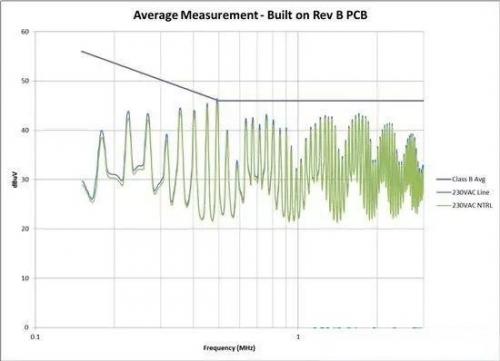
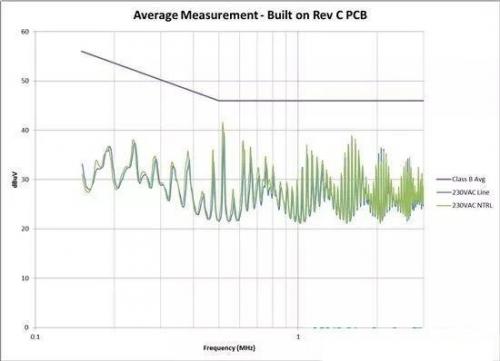
|
The OP
Published on 2019-7-21 22:35
Only look at the author
This post is from Analogue and Mixed Signal
| ||
|
|
||
- 【Posts】The impact of common mode noise on EMI
- 【Posts】How to distinguish between differential mode noise and common mode noise?
- 【Posts】About EMC, spectrum basics, differential mode noise and common mode noise
- 【Posts】What kind of noise is the ripple generated by the power chip? Common mode noise or differential mode noise?
- 【Posts】The high end samples a current, the common mode voltage is up to 250v, and the frequency is max500khz. Is there a suitable pre-amplifier?
- 【Posts】How to use common mode inductors?
- 【Posts】Can common-mode inductors and differential-mode inductors be used for DC filtering?
- 【Posts】Multisim noise simulation and noise coefficient simulation issues
- 【Download】Common Mode Rejection and EMI Interference
- 【Download】EMI and its common mode inductance
- 【Download】Research on common mode EMI suppression technology of switching power supply.rar
- 【Download】Analysis of Inductor EPC and Improvement of Common Mode Insertion Loss in Integrated EMI Filter
- 【Download】Low noise design of Tektronix MSO6 and several common methods to reduce noise on display signals
- 【Download】EMI Debugging Practices
- 【Download】Audio test source: pink noise and 1KHz sine wave (MP3, 0dB)
- 【Download】Noise and Power Consumption of IoT Smart Sensors
- 【Design】LM317+LM337 headphone amplifier power board (onboard transformer and EMI circuit)
- 【Design】M1 EMI filter
- 【Design】DM9000 EMI test circuit reference
- 【Design】3W non-isolated bias power supply reference design with 80% efficiency and 15dB EMI performance margin
- 【Design】5V 1A, low EMI, 94% efficiency DC/DC module reference design using double-layer TO-220 package
- 【Design】3.3V 1A, low EMI, 92% efficiency DC/DC module reference design in double-layer TO-220 package
- 【Circuits】What is the impact between power supply noise and high-speed DAC phase noise?
- 【Circuits】Utilizing light sensing circuits to reduce photodiode bandwidth and noise effects
- 【Circuits】Common-mode voltage breakdown of op amp input stage and its protection measures
- 【Circuits】A differential amplifier with a common mode voltage up to ±1000V composed of INA110
- 【Circuits】Measurement amplifier circuit with high common-mode range
- 【Circuits】Anti-common mode transient interference circuit
- 【Articles】Common Mode Semiconductor Launches GM2500, a Small, High-Efficiency, Low-EMI, Synchronous 6A Step-Down Converter Based on Turbo Switch Technology
- 【Articles】How to reduce the size of common mode choke? Active EMI filter ICs available
- 【Articles】Standalone Active EMI Filter IC How to Reduce Common Mode Filter Size
- 【Articles】Wayon launches the first ESD&EMI product integrating silicon-based common mode filtering and electrostatic protection
- 【Articles】Two aspects to quickly distinguish differential mode and common mode in EMI testing
- 【Articles】EMI common mode current measurement using an oscilloscope
-
What kind of noise is the ripple generated by the power chip? Common mode noise or differential mode noise?
Whatkindofnoiseistheripplegeneratedbythepowerchip
-
How to select common mode inductors and differential mode inductors for circuit boards to suppress EMC and EMI
TheinputvoltageisDC24V,andthecircuitboardcurrentisrelativelysmall,onlyabout20mA
-
Xiaomi's four-motor system can make a compass turn and turn on the spot. Is it difficult to implement the algorithm?
Isthefour-motorcompassturnandon-the-spotturnjustanincreaseincost,oristhereabreakthroughinthealgorithmNow,manypeopleareamazedbythefeaturesshownbyXiaomi'sintelligentchassispre-researchvehicleI'mwaitingforforumfriendstohelpmesolvemydoubts.
- GPS spoofing has become a global problem, but how can we solve it?
- Advanced Designer 25.0.2
- Unboxing Review
- Supplementary information on the two disassembled isolators and detailed disassembly pictures
- MCU reset problem
- Please advise on PMOS high-side driver under wide voltage range!
- LIS2MDL array magnet displacement data acquisition for magnetic nail navigation AGV
EEWorld Datasheet Technical Support
-
Qualcomm launches its first RISC-V architecture programmable connectivity module QCC74xM, supporting Wi-Fi 6 and other protocols
On November 14, Qualcomm announced the launch of two connectivity modules, QCC74xM and QCC730M, f
-
It is reported that memory manufacturers are considering using flux-free bonding for HBM4 to further reduce the gap between layers
On November 14, according to Korean media ETNews, Samsung Electronics, SK Hynix, and Micron are a
-
ON Semiconductor CEO Appears at Munich Electronica Show and Launches Treo Platform
During Electronica, ON Semiconductor CEO Hassane El-Khoury was interviewed by Power Electronics N
- AMD launches second-generation Versal Premium series: FPGA industry's first to support CXL 3.1 and PCIe Gen 6
- SEMI: Global silicon wafer shipment area increased by 6.8% year-on-year and 5.9% month-on-month in 2024Q3
- TSMC's 5nm and 3nm supply reaches "100% utilization" showing its dominance in the market
- LG Display successfully develops world's first stretchable display that can be expanded by 50%
- Seizing the Opportunities in the Chinese Application Market: NI's Challenges and Answers
- New diaphragm-free solid-state lithium battery technology is launched: the distance between the positive and negative electrodes is less than 0.000001 meters
- Photoresist giant JSR Korea EUV MOR photoresist production base started construction, expected to be put into production in 2026
- Problems with STM32 and passive buzzer playing sound
- Embedded Tutorial_DSP Technology_DSP Experiment Box Operation Tutorial: 2-28 Building a Lightweight WEB Server Experiment
- OPA847IDBVR op amp domestic replacement
- AG32VF407 Test UART
- [Digi-Key Follow Me Issue 2] Chapter 1: Sharing on receiving the goods
- What model is this infrared receiver? Which model can be used instead? Thank you
- Selling brand new unopened ZYNQ 7Z020 FPGA core board
- The LORA module used in the lithium battery-powered water meter setting can save energy when 100 water meters are installed in one corridor.
- I would like to ask, when a port is set to RX0, is it necessary to set the input and output direction of this port?
- Why is this year so difficult? It’s even more difficult than during the pandemic. I’m 30 and facing unemployment. I’m so confused.
- Ask about the voltage regulator test question
- [Xiaohua HC32F448 Review] About Xiaohua Semiconductor's UART interrupt sending and PRINTF construction and redirection
- 【BIGTREETECH PI development board】 HDMI output test
- 【BIGTREETECH PI development board】+08. Audio test (zmj)
- [Xiaohua HC32F448 Review] +RTC electronic clock
- # STM32H7S78-DK Development Kit Three-week Review: Implementation and Analysis of Simple Sound Collection and Storage Using SD Card Reading and Writing
- [STM32H7R/S] Review⑧ nano edge ai studio training a model--Part 1
- [2024 DigiKey Creative Competition] A "fortune-telling" artifact based on Raspberry Pi
- New energy vehicle on-board AC slow charging and maintenance
- Embedded Engineer AI Challenge Camp (Advanced): Deploy InsightFace algorithm on RV1106 for real-time face recognition of multiple people
- I want to make a self-driving car. I saw one on Bilibili that costs 300 yuan. I am hesitant.
- [K230 Embedded AI Development Board Review] + License Plate Recognition and Billing Management
- How to deploy LVGL free graphics library on low-cost ARM platform, based on Allwinner T113-i
- Please help me analyze the reasons why EMI fails.
- ChatTTS is really awesome!
- 参会有好礼 | 2024 瑞萨电子MCU/MPU工业技术研讨会
- 深圳站:11月30日(周六)深圳湾万怡酒店
上海站:12月06日(周五)上海喜玛拉雅酒店
奖励设置:现金红包、螺丝刀套装或30元京东卡
- Littelfuse 新品赋能电子产品安全可靠并高效, 10+挑战等你探索!
- Littelfuse 应用赋能星球,覆盖了诸多应用痛点及解决办法,邀请工程师一起探索,解锁更多设计力!
- 了解英飞凌新品AIROC™ CYW5591x 无线MCU,答题赢好礼!
- 无线键盘鼠标套装、智能音箱、登山包、收纳包
- 下载资料赢好礼!看Vicor模块化电源解决方案如何推动创新
- 活动时间:即日起-2024年12月31日
如何参与:点击活动页内您想了解的模块,找到资料下载即可参与抽奖,活动结束后统一发奖!
- 有奖活动|英飞凌高密度双相电源模块为高性能运算平台而生
- 活动时间:即日起-12月15日
活动奖励:蓝牙音箱、氮化镓充电器套装、黑色小背包
- 本周精选下载推荐:电源管理基础Dummies
- 本周小编给大家带来一本超简单、超干货的电子书——《电源管理基础Dummies》!内容深入浅出,排版舒服简洁,分分钟能get到电源管理最核心的知识内容。
EEWorld
subscription
account

EEWorld
service
account

Automotive
development
circle

About Us Customer Service Contact Information Datasheet Sitemap LatestNews
- I want to get started with machine learning with pytjon, what should I do?
- For the introduction to fpga logic, please give a study outline
- For an introduction to big data machine learning, please give a study outline
- For the introduction to mobile phone microcontroller programming, please give a learning outline
- For hardware microcontrollers, please give a study outline
- How long does it take to get started with FPGA?
- What to learn first when getting started with SMT programming
- How to get started learning to make robots
- How to quickly get started with deep learning
- What FPGA development board is suitable for beginners?


 Room 1530, Zhongguancun MOOC Times Building,
Block B, 18 Zhongguancun Street, Haidian District,
Beijing 100190, China
Tel:(010)82350740
Postcode:100190
 京公网安备 11010802033920号


 提升卡
提升卡 变色卡
变色卡 千斤顶
千斤顶