TMS320F2812 is a 32-bit high-performance digital signal processor (DSP) with a main frequency of up to 150 MHz launched by Texas Instruments (TI), which integrates an ADC conversion module. The ADC module is a 12-bit analog-to-digital converter with a pipeline structure, built-in dual sample-and-hold (S/H), and can select 16 channels of input. The fast conversion time runs at 25 MHz, ADC clock or 12.5 Msps, and the 16 conversion result registers can work in continuous automatic sorting mode or start/stop mode.
In modern electronic systems, as a key component of the interface between analog systems and digital systems, the analog-to-digital converter (ADC) has become a very important circuit unit for data acquisition in control loops. In actual use, it is found that the conversion result of the ADC has a large error. If this conversion result is directly used in the control loop, the control accuracy will inevitably be reduced. In order to overcome this shortcoming and improve its conversion accuracy, the author proposed a method for improving the accuracy of TMS320F2812 ADC after conducting a large number of experiments, which effectively improved the ADC accuracy.
1 Definition and Impact Analysis of ADC Module Error
1.1 Error Definition
Commonly used A/D converters mainly have: offset error, gain error and linearity error. Here we mainly discuss offset error and gain error. Ideally, the conversion equation of the ADC module is y=x×mi, where x=input count value=input voltage×4095/3; y=output count value. In practice, various errors of the A/D conversion module are inevitable. Here, the conversion equation of the ADC module with gain error and offset error is defined as y=x×ma±b, where ma is the actual gain and b is the offset error. After multiple measurements of the ADC signal acquisition of F2812, it was found that the ADC gain error is generally within 5%, that is, 0.95
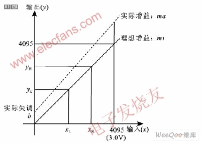
Figure 1 Ideal ADC conversion and actual ADC conversion
1.2 Impact Analysis
In computer measurement and control systems, the acquisition of object data generally includes two basic physical quantities: analog quantity and digital quantity. Computers can read digital quantities directly, while analog quantities can only be accepted by computers after being converted into digital quantities. Therefore, in order to accurately acquire and process analog quantities, the precision and accuracy of analog-to-digital conversion must meet certain requirements. Since the ADC of F2812 has a certain gain error and offset error, it is easy to cause system misoperation. The following analyzes the impact of the two errors on linear voltage input and A/D conversion results.
The ADC module input analog voltage provided in the F2812 user manual is 0 to 3 V. However, in actual use, due to the existence of gain error and offset error, its linear input is reduced. The analysis is listed in Table 1.
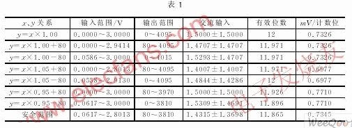
The following uses y=x×1.05+80 as an example to introduce the calculation of each value. When the input is 0, the output is 80. Since the maximum output value of the ADC is 4095, the maximum input voltage value is 2.8013 obtained by the formula y=x×1.05+80. Therefore, the AC input voltage range is 1.4007±1.4007, and the effective number of bits N=ln4015/ln2=11.971, mV/count bit=2.8013/4015=0.6977. The calculation of the remaining items is the same as above. The last row in Table 1 shows the safety parameters of the ADC operation. The effective number of bits is reduced to 11.865 bits, and the mV/count bit is increased from 0.7326 to 0.7345, which will reduce the conversion result by 0.2%.
In practical applications, the collected signals are often bipolar signals, so a conversion circuit needs to be added before the signal is sent to the ADC to convert the bipolar signal into a unipolar signal. A typical conversion circuit is shown in Figure 2. For the ADC module, considering the impact of gain error and offset error on the input range, the conversion circuit needs to be adjusted to the circuit shown in Figure 3. In Figure 3, the reference range of the input gain error has been changed.
For bipolar input, the gain error of 0 V input corresponds to the gain error of 1.4315V of unipolar input, so the gain error and offset error of the original ADC are increased. For example, if the gain error of the ADC is 5% and the offset error is 2%, the bipolar gain error is calculated as follows: bipolar input x′= 0.0000 V, unipolar ADC input voltage x = 1.4315 V, its ideal conversion value is ye=1.4315×4095/3=1954, and the actual conversion value is calculated by ya=1954×1.05+80, then the bipolar gain error is ya-ye=2132-1954=178 (9.1% error). It can be seen from the calculation that the error of the ADC is greatly increased, so if you want to use the ADC for data acquisition, you must calibrate the ADC to improve its conversion accuracy.
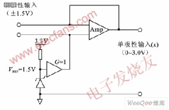
Figure 2 Ideal voltage conversion circuit
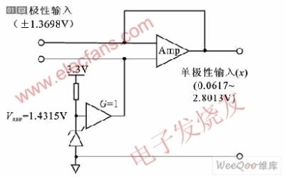
Figure 3 Corrected voltage conversion circuit
2 ADC Calibration
2.1 Calibration method
From the above analysis, we can see that the main reason for the poor ADC conversion accuracy of F2812 is the existence of gain error and offset error. Therefore, to improve the conversion accuracy, the two errors must be compensated. The following method is adopted to correct the ADC module.
Select any two channels of the ADC as reference input channels, and provide them with known DC reference voltages as inputs (the two voltages cannot be the same), obtain the conversion values by reading the corresponding result registers, and use the two sets of input and output values to obtain the correction gain and correction offset of the ADC module, and then use these two values to compensate for the conversion data of other channels, thereby improving the accuracy of the ADC module conversion. Figure 1 shows how to use the equation to obtain the correction gain and correction offset of the ADC. The specific calculation process is as follows:
① Obtain the conversion values yL and yh of the known input reference voltage signal.
② Use the equation y = x × ma + b and the known reference values (xL, yL) and (xH, yH) to calculate the actual gain and offset errors:
Actual gain ma=(yH-yL)/(xH-xL);
Offset error b="yL" -xL×ma.
③ Define the input x=y×CalGain-CalOffset, then from the equation y=x×ma+b, we can get the correction gain CalGain=1/ma=(xH-xL)/(yH-yL), and the correction offset CalOffset=b/ma=yL/ma-xL.
④ Apply the required correction gain and correction offset to other measurement channels to correct the ADC conversion results.
The above is the whole process of ADC correction. By using this method, the conversion accuracy of ADC is greatly improved. Since this method uses the error of a certain channel to correct the error of other channels, it is necessary to ensure that there is a small channel error between channels to use this method. For the F2812ADC conversion module, since the gain and offset errors between its channels are within 0.2%, this method can be used to correct it.
2.2 Software Implementation
Compared with the general ADC conversion program, the ADC conversion program with correction needs to add two additional program segments: calculation of the correction value and processing of the ADC using the correction value. In order to facilitate the operation and acquisition of the conversion results, the structure variable ADC-CALIBRATION-VARS is defined in the implementation to save various data after ADC conversion. In addition, to improve the versatility of the program, the sampling method, reference voltage value and ideal conversion values of high and low voltages are all defined in the ADC conversion header file ADCCalibration.h.
ADC-CALIBRATION-VARS are defined as follows:
typedefstruct{
Uint*RefHighChAddr; //reference high voltage connected channel address
Uint*RefHighChAddr; //reference low voltage connected channel address
Uint*ChoAddr; //0 channel address
UintAvg_RefHighActualCount; //Reference high voltage actual conversion value
UintAvg_RefHighActualCount; //Reference low voltage actual conversion value
UintRefHighIdealCount; //Reference high voltage ideal conversion value
UintRefLowCount; //Reference low voltage actual conversion value
UintCalGain; //Correction gain
UintCalOffset; //correction offset
//Correction channel conversion value
UintCh0;
UintCh16;
}ADC CALIBRATION VARS;
The entire A/D conversion task consists of the interrupt function intADC() and the main function ADCCalibration(). The interrupt function is mainly used to read the conversion data, while the correction parameter calculation and the correction of the conversion results of each channel are completed in the main function. After the correction, the result is saved in the defined structure variable. Here, the ADC correction adopts the single sampling and single correction processing method. Of course, the multi-sampling and single correction processing method can also be used. However, in order to improve the accuracy, if the design system cost allows, it is recommended to use the single sampling and single correction method to improve the ADC accuracy.
2.3 Experimental Results
The author conducted an experiment on the F2812 system he used, selecting 1 V and 2 V as reference voltages, and channels A6 and A7 as reference channels. By comparing the data before and after correction of 0 V, 0.5 V, 1.5 V, and 2.5 V, it was found that the conversion accuracy of the ADC was significantly improved after adopting the above correction method. The comparison results are listed in Table 2.
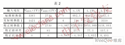
Note: Calculated from the reference voltage: CalGain=0.965; CalOffset=6.757.
The data given in Table 2 are only a set of data obtained by the author after a large number of experiments. The experiments show that the error of the ADC can be controlled within 0.5% after correction, which meets the requirements for most measurement and control systems. For systems with higher conversion accuracy requirements, an external A/D converter can be used.
Conclusion
A/D converter is the core component of data acquisition circuit, and its good precision and accuracy are the key to improving the performance of data acquisition circuit. TMS320F2812 is a 32-bit processor launched by TI that integrates microcontroller and digital signal processor. It is widely used for its high running speed and powerful processing function. The improvement of its ADC module accuracy will further improve its application in the control field. The correction algorithm proposed in this paper for improving the accuracy of ADC module has been proved to be practical and feasible through practical application.


 Modern Compiler Principles C Language Description (Ampel)
 ESP32-S3 source code
 【Follow me Season 2 Episode 2】Arduion UR4 homework submission code


 京公网安备 11010802033920号