In the deep submicron era, traditional materials, structures and even processes are reaching their limits, and Moore's Law is already somewhat stretched. Entering the deep subnanometer era, the size of transistors will be close to that of a single atom and cannot be reduced any further. Traditional ASIC and ASSP designs inevitably encounter problems such as complex design processes, reduced production yields, long design cycles, and a sharp increase in R&D and manufacturing costs, which to some extent have greatly slowed down the continuation of Moore's Law.


Keywords:FPGA
Reference address:FPGA+CPU: Parallel processing is popular
It is obvious that facing the huge tape-out costs, many small and medium-sized companies have to change their strategies and turn more to FPGA development and design. Looking at the FPGA market, even five years ago, its market growth rate was still quite slow compared to ASIC, but in recent years, especially after entering the 90nm node, its cost advantage has gradually become prominent.
For 20 years, Xilinx and Altera, the two giants that have long dominated the programmable logic device market, have been making frequent moves. In August, Altera held a seminar and a technical tour in 13 cities, vigorously promoting V series products on the 28nm process, the transition from SOPC Builder to the new Qsys platform, and even the new concept of SOC FPGA. In contrast, Xilinx was much more low-key in September, but still took out the 7 series products to challenge its competitors. From 65nm a year ago to 28nm today, since gate delay is no longer a bottleneck for speed performance improvement, the only change that users can feel is the increase in device density and the decrease in unit cost. In addition, it can only be said that manufacturers racking their brains to optimize device architecture and improve development tool performance has become another landscape to watch.
Coincidentally, Xilinx and Altera have accelerated the launch of FPGA devices with embedded hard-core CPUs. The FPGA+CPU solution is not uncommon. It was proposed and put into practice as early as five years ago. Xilinx and Altera have also been committed to the promotion of their own soft-core CPUs, but the market response has obviously not met expectations. In response to market demand, Xilinx took the lead in releasing the Extensible Processing Platform architecture integrating ARM Cortex-A9 CPU and 28nm FPGA in April last year. Less than a year later, the extensible processing platform Zynq-7000 series has been brought to the forefront again, which shows Xilinx's good intentions. Altera is not to be outdone. Intel integrated Altera's FPGA into the Atom E600C configurable processor released last fall, and Altera's upcoming SoC FPGA, which also integrates the Cortex-A9 CPU, is obviously intended to compete with Xilinx.
For us, we need to explore and think whether this new development platform can really meet the growing "material culture" needs of customers. We can't help but ask: Is the FPGA+CPU integrated architecture in line with the trend of historical development, or is it just a flash in the pan?
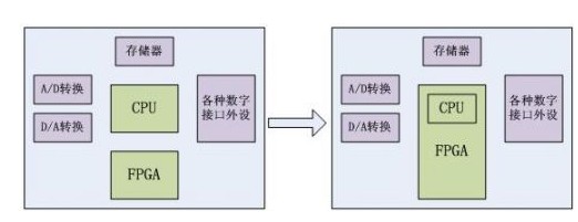
As shown in Figure 1, a relatively simplified traditional embedded system is shown on the left, and the FPGA architecture with a single integrated CPU is shown on the right. From the perspective of hardware architecture alone, it does not seem to have much advantage, it is just two-in-one. However, engineers who have actually done system development know that this two-in-one brings not only BOM cost reduction and layout simplification, but also more benefits such as optimization of the underlying connection between software and hardware that is invisible to the naked eye, and the invisible flexibility and potential performance improvement.

figure 1
Some potential advantages of FPGA-based CPU integration include: easier to meet the functional requirements of most systems; potential improvement in system performance; greatly improved flexibility and upgradeability in certain applications; optimized processor-to-peripheral interface; greatly improved interface performance for hardware and software interconnection; conducive to design reuse and rapid prototyping of new designs; and simplified PCB layout and routing for single chips or even entire boards.
The advantages of FPGA+CPU monolithic integration over traditional applications are evident from this, but from another perspective, just as the evolution of CPU from single-core to multi-core is continuing the "curse" of Moore's Law, the strong attack of FPGA+CPU is more like the popularity of parallel processing in embedded applications.
Continuing their usual style, Xilinx and Altera have both chosen the excellent ARM Cortex-A9 core for their CPU-embedded FPGA devices, which shows that they are currently targeting the mid-to-high-end application customers. As for low-end applications, even in the era of Internet explosion, the obscure Capital-Micro company is still not well known to the majority of engineers, but the reconfigurable system chip CsoC (Configurable SoC) they developed has quietly carved out a bloody path in the mid-to-low-end market applications. It is worth mentioning that this is a genuine Chinese local FPGA manufacturer.
It has been exactly 40 years since Intel's first 4-bit processor was launched in 1971. Although the embedded industry has undergone tremendous changes, even if you think it is "rustic" but simple and practical, the 8-bit MCS-51 microcontroller is still unique, especially in the entire domestic industrial control industry. Since its establishment in 2005, Capital-Micro has successively launched two generations of CSoC, Astro and AstroII. Its embedded 8051 can run stably at 100MHz and 150MHz on the two generations of devices respectively. Although the FPGA manufacturing process is still at 0.13um, which greatly restricts the logic performance, the current two generations of products can at least meet the industrial application needs including stepper motor control, LCD drive control, interface expansion, LED control card, and micro printer.
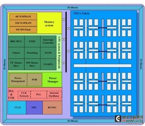
From the internal architecture of the device, as shown in Figure 2, AstroII not only has the 8051 hard core with "excellent" performance among similar products, but also integrates some common peripherals such as timers, watchdogs, UARTs, IICs and SPIs. Of course, the program startup of 8051 also completely adopts a direct mapping (Fully Shadowed) method similar to many ARMs to ensure that the slow reading and writing of ROM no longer becomes a bottleneck restricting CPU performance. As for the interconnection between 8051 and FPGA, not only can the EMIF addressing of 8051 (23-bit wide addressable address bus) be used, but the 4K×8bit DPRAM is also a good choice for high-speed data transmission, and the synchronization logic has been solidified on these interconnection interfaces, without the need for designers to waste energy. In addition, from the cheapest crystal clock support to the maximization of the number of I/Os, to its affordable price, all show us the "economical and practical" nature of this domestic chip.

figure 2
In a word, no matter it is Xilinx, Altera, or the emerging Capital-Micro, the new monolithic integrated devices they promote all indicate that the parallel processing architecture of FPGA+CPU will open up a brand new world in embedded applications. In this deep sub-nanometer era where the performance improvement of single chip is about to reach its limit, the flexible and changeable FPGA will surely help the performance of traditional CPU to reach new heights again with its unique parallelism.
Previous article:TMS320C6678 Memory Access Performance (Part 1)
Next article:VLFFT Demonstration for TMS320C6678 Processor
Recommended ReadingLatest update time:2024-11-16 14:29
NVIDIA Announces CPU for Massive AI and High-Performance Computing Workloads
The “Grace” CPU uses energy-efficient Arm cores to deliver a 10x performance boost for systems training giant AI models Swiss Supercomputer Center and U.S. Department of Energy’s Los Alamos National Laboratory Build First Supercomputer Powered by NVIDIA CPUs SANTA CLARA, Calif. — GTC — April 12, 2021 — NVIDIA un
[Network Communication]
Design of a Simple DDS Signal Generator Based on FPGA

Preface DDS is the abbreviation of Direct Digital Synthesizer, which is a key digital technology. Compared with traditional frequency synthesizers, DDS has the advantages of low cost, low power consumption, high resolution and fast conversion time. It is widely used in the field of telecommunications and electronic in
[Test Measurement]

High-performance DC/DC converters meet power supply requirements in FPGA applications

As FPGA manufacturing process size continues to shrink, design configuration becomes more flexible, and systems using FPGAs continue to evolve, applications that were previously only available with microprocessors and ASICs can now be implemented with FPGAs. New programmable devices recently introduced by FPGA vendors
[Power Management]

Design and implementation of digital fluxgate sensor system based on FPGA

introduction
The fluxgate sensor was first invented and put into use in 1935. It is used for static or low-frequency weak magnetic detection. It has a sensitivity and reliability that is difficult to match with other magnetic sensitive components. It has always occupied an irreplaceable position in the field of magn
[Embedded]

Design of Network Image Acquisition and Processing System Based on FPGA

1 Overall Design The overall block diagram is shown in Figure 1. The system uses the StratixⅡ series EP2S60F484 model FPGA launched by Altera as the core of image acquisition processing and network transmission. The video A/D uses the ADV7181B chip, which supports PAL, NTSC and SECAM video input. Image acquisition pr
[Microcontroller]

Ni Guangnan: RISC-V has become China’s first choice for CPU architecture in many fields
The 2023 RISC-V China Summit (RISC-V Summit China 2023) will be held in Beijing from August 23 to 25. With the theme of "RISC-V ecological co-construction", this summit conducted an in-depth discussion on the development of RISC-V industry. Ni Guangnan, academician of the Chinese Academy of Engineering, pointed out in
[Embedded]
Design of Mud Electrical Parameters Measurement System Based on FPGA

introduction
my country has a vast geographical area and rich natural resources. Among them, oil is the blood of my country's industry and an important energy source that supports the rapid development of my country's economy. It is related to national energy security and social stability . However, the process of oil
[Test Measurement]

Open FPGA increases test flexibility

Most instruments today use closed FPGAs (field programmable gate arrays) and fixed firmware to implement instrument functionality. If you’ve ever seen an oscilloscope disassembled, you’ve probably seen the FPGA inside. FPGAs can add processing power to test instruments, and if you’ve ever used an instrument with an ope
[Test Measurement]

- Popular Resources
- Popular amplifiers
-
 Analysis and Implementation of MAC Protocol for Wireless Sensor Networks (by Yang Zhijun, Xie Xianjie, and Ding Hongwei)
 -
 MATLAB and FPGA implementation of wireless communication
 -
 Siemens PLC Programming Technology and Application Cases (Edited by Liu Zhenquan, Wang Hanzhi, Yang Kun, etc.)
 -
 Siemens PLC from Beginner to Mastery with Color Illustrations (Yang Rui)
Recommended Content
Latest Embedded Articles
- Huawei's Strategic Department Director Gai Gang: The cumulative installed base of open source Euler operating system exceeds 10 million sets
- Analysis of the application of several common contact parts in high-voltage connectors of new energy vehicles
- Wiring harness durability test and contact voltage drop test method
- Sn-doped CuO nanostructure-based ethanol gas sensor for real-time drunk driving detection in vehicles
- Design considerations for automotive battery wiring harness
- Do you know all the various motors commonly used in automotive electronics?
- What are the functions of the Internet of Vehicles? What are the uses and benefits of the Internet of Vehicles?
- Power Inverter - A critical safety system for electric vehicles
- Analysis of the information security mechanism of AUTOSAR, the automotive embedded software framework
He Limin Column
Microcontroller and Embedded Systems Bible
 Professor at Beihang University, dedicated to promoting microcontrollers and embedded systems for over 20 years.
MoreSelected Circuit Diagrams
MorePopular Articles
- Innolux's intelligent steer-by-wire solution makes cars smarter and safer
- 8051 MCU - Parity Check
- How to efficiently balance the sensitivity of tactile sensing interfaces
- What should I do if the servo motor shakes? What causes the servo motor to shake quickly?
- 【Brushless Motor】Analysis of three-phase BLDC motor and sharing of two popular development boards
- Midea Industrial Technology's subsidiaries Clou Electronics and Hekang New Energy jointly appeared at the Munich Battery Energy Storage Exhibition and Solar Energy Exhibition
- Guoxin Sichen | Application of ferroelectric memory PB85RS2MC in power battery management, with a capacity of 2M
- Analysis of common faults of frequency converter
- In a head-on competition with Qualcomm, what kind of cockpit products has Intel come up with?
- Dalian Rongke's all-vanadium liquid flow battery energy storage equipment industrialization project has entered the sprint stage before production
MoreDaily News
- Allegro MicroSystems Introduces Advanced Magnetic and Inductive Position Sensing Solutions at Electronica 2024
- Car key in the left hand, liveness detection radar in the right hand, UWB is imperative for cars!
- After a decade of rapid development, domestic CIS has entered the market
- Aegis Dagger Battery + Thor EM-i Super Hybrid, Geely New Energy has thrown out two "king bombs"
- A brief discussion on functional safety - fault, error, and failure
- In the smart car 2.0 cycle, these core industry chains are facing major opportunities!
- The United States and Japan are developing new batteries. CATL faces challenges? How should China's new energy battery industry respond?
- Murata launches high-precision 6-axis inertial sensor for automobiles
- Ford patents pre-charge alarm to help save costs and respond to emergencies
- New real-time microcontroller system from Texas Instruments enables smarter processing in automotive and industrial applications
Guess you like
- stm32f030R8 Chinese reference material
- Recruitment: Executive Vice President of Automotive Electronics (Executive Vice President of New Energy)
- ATmega4809 Curiosity Nano Review + Unboxing and Powering on
- Sell an unused Jiuxintaike oscilloscope and get a Guwei desktop multimeter for free
- MSP430F1232 external 4M crystal oscillator cannot start
- PCB connector connection method
- Using STM32F103 as Arduino
- What are the two MOS tubes used for in the feedback circuit of the Boost circuit?
- EEWORLD University Hall----Inverter Principle and Application Harbin Institute of Technology
- Weekly highlights: 2018.11.12-2018.11.18

 Analysis and Implementation of MAC Protocol for Wireless Sensor Networks (by Yang Zhijun, Xie Xianjie, and Ding Hongwei)


 京公网安备 11010802033920号