1 Circuit Design
1.1 Design Principle
DDS directly excites the frequency synthesis technology of PLL. Compared with the pure PLL technology, DDS as a reference source has a very high frequency resolution. It can improve the frequency resolution of PLL without changing the PLL division ratio. In addition, the circuit structure of the DDS excitation PLL design method is simple, and the hardware used is small. The phase noise deteriorated by the PLL frequency multiplication can be improved by properly designing the loop filter. The system principle block diagram is shown in Figure 1.

In Figure 1, fref is the reference signal, which is generally generated by a high-stability crystal oscillator to ensure the synchronous operation of each component of DDS. fDDS replaces the original crystal oscillator as the excitation source of the phase-locked loop (PLL), and its output fDDS frequency depends on the frequency control word K. The output of the frequency synthesizer is provided by the VCO, and the output of the charge pump in the PLL chip is generated by the low-pass filter (LPF2) to control the output frequency of the VCO. The K in the DDS and the division ratio of the PLL can be changed by the control program in the microcontroller to achieve frequency synthesis.
The relationship between the VCO output signal frequency and the DDS output signal frequency is:
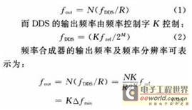
Where: fref is the clock frequency of DDS; K is the frequency control word of DDS; M is the word length of DDS phase accumulator; fref/2M is the frequency resolution of DDS; △fmin is the frequency resolution of the frequency synthesizer output signal. It can be seen that with DDS as the excitation source, as long as the word length of the phase accumulator is large enough, the frequency synthesizer can obtain a higher frequency resolution.
1.2 Circuit Implementation
As shown in the principle block diagram given in Figure 1, the entire frequency synthesizer is implemented by two functional modules, DDS and PLL.
1.2.1 DDS Circuit
The DDS circuit is shown in Figure 2. The circuit consists of DDS, low-pass filter (LPF) and external reference clock source. The direct digital frequency synthesizer chip AD9851 in the circuit is a highly integrated DDS device produced by AD using advanced DDS technology. It allows a maximum input clock of 180 MHz, while providing an optional on-chip 6-fold frequency multiplier, built-in high-performance 10 The chip has a simple control interface, allowing serial/parallel asynchronous input of control words, using 32 b frequency control words, and using 5 b phase modulation words internally. When an external reference clock source is connected, AD9851 can generate a sine wave with pure spectrum, controllable frequency and phase, and very high stability.
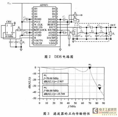
This paper uses the single-chip microcomputer C8051F021 to control the AD9851 data. By changing the operation mode selected by the internal programming control register of AD9851, the number of bits of the phase accumulator, and the frequency control word, the output of various frequency signals can be realized. The external reference clock source uses a 30 MHz passive crystal oscillator, and the frequency of the DDS output signal can reach up to 72 MHz. The external low-pass filter is used to filter out high-frequency spurious and harmonics.
DDS has a very obvious disadvantage. The closer the output frequency is to the height of the Nyquist bandwidth, the fewer the number of sampling points, and the greater the spurious interference of its output. Therefore, a filter must be added to the sine signal output end of the DDS chip to effectively suppress harmonics and spurious. In this design, a seventh-order elliptic low-pass filter is used. The filter circuit is shown in the dotted box in Figure 2, where R5 and R6 complete the conversion of current signal to voltage signal, and its cutoff frequency can reach 70 MHz. Figure 3 shows the forward transmission characteristics of the seventh-order elliptic low-pass filter. The attenuation at the 70 MHz cutoff frequency is -2.907 dB, and the out-of-band attenuation reaches -35.749 dB at 84 MHz, which basically meets the design requirements.
1.2.2 PLL circuit
The PLL circuit is shown in Figure 4. The circuit consists of a highly cost-effective phase-locked chip ADF4113, a filter circuit, and VC0. In the design, DDS output is used to replace the original crystal oscillator to provide a 13 MHz excitation source for the GSM system. The channel frequency interval is 200 kHz, and the reference input needs to be divided by 65 by the reference divider in ADF4113.
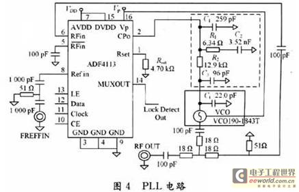
ADF4113 is a digital phase-locked frequency synthesizer developed by ADI. The maximum operating frequency can reach 4 GHz. It can be used in base stations, mobile phones, communication detection equipment and CATV equipment in wireless RF communication systems. The chip mainly includes a programmable 14-bit reference divider; a programmable dual-mode pre-divider: 8/9, 16/17, 32/33 and 64/65; a programmable RF signal divider; a 3-wire serial bus interface; and analog and digital lock state detection functions. The chip has good phase noise parameters. When the phase detection frequency is 200 kHz, the phase noise floor is -164 dBc/Hz; when the output is 1 840 MHz, the phase noise can reach -85 dBc/Hz. The VCO uses Sirenza Microwave's VC0190-1843T, with an output frequency range of 1 740 to 1 930 MHz. It has good phase noise characteristics, and its unique buffer amplifier design can reduce frequency drift. The
loop filter has a very important influence on the performance of the frequency synthesizer. The loop filter determines important parameters of the frequency synthesizer, such as spurious suppression, phase noise, loop stability, and agility time. Since this design uses the ADF4113 current-type charge pump phase detector, the loop filter adopts a passive method. Since the switching time requirement for frequency hopping is not very high in this system, the loop bandwidth can be appropriately reduced to ensure the stability of the system. Reducing the loop bandwidth also helps to filter out the harmonic components in the reference signal. However, if the loop bandwidth is too small, the settling time and the in-band VCO phase noise will increase. Since the in-band noise mainly depends on the noise introduced by the reference signal, the VC0 phase noise is not the main factor. The system is designed as a fourth-order loop composed of a third-order passive filter. The dotted box in Figure 4 shows the third-order passive loop filter circuit. According to the system's requirements for phase noise and frequency conversion time, the loop bandwidth ωc=15 kHz and the phase margin φ=45° are taken.
2 Circuit Simulation
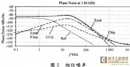
The ADISimPLL software was used to simulate and analyze the solution, and Figure 5 shows the simulation results. It can be seen that the phase noise of the frequency synthesizer is -84.63 dBc/
3 Results Analysis
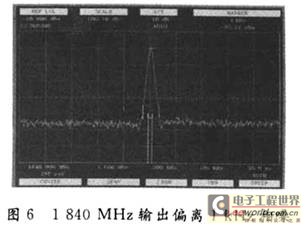
The system adopts the design of DDS direct excitation PLL, making full use of the advantages of DDS small step, fast frequency agility and PLL wide frequency band, high operating frequency and high spectrum purity, and develops a frequency synthesizer that meets the requirements of GSM 1 800 MHz system indicators. The measurement of phase noise is shown in Figure 6, which is -83.75 dBc/
4 Conclusion
The frequency synthesis technology of DDS excitation PLL overcomes the shortcomings of low DDS output frequency and low PLL frequency resolution in broadband systems. By reasonably designing the loop low-pass filter, phase noise, loop stability and other performances are improved, and filtering measures are taken on the power supply to improve clutter suppression, and finally a high-performance frequency synthesizer is designed.
Previous article:Digital signal controllers provide real-time control capabilities
Next article:OMAP5910 Embedded System Based on ARM Core and DSP Core
Recommended ReadingLatest update time:2024-11-16 14:27


- Huawei's Strategic Department Director Gai Gang: The cumulative installed base of open source Euler operating system exceeds 10 million sets
- Analysis of the application of several common contact parts in high-voltage connectors of new energy vehicles
- Wiring harness durability test and contact voltage drop test method
- Sn-doped CuO nanostructure-based ethanol gas sensor for real-time drunk driving detection in vehicles
- Design considerations for automotive battery wiring harness
- Do you know all the various motors commonly used in automotive electronics?
- What are the functions of the Internet of Vehicles? What are the uses and benefits of the Internet of Vehicles?
- Power Inverter - A critical safety system for electric vehicles
- Analysis of the information security mechanism of AUTOSAR, the automotive embedded software framework
 Professor at Beihang University, dedicated to promoting microcontrollers and embedded systems for over 20 years.
- Innolux's intelligent steer-by-wire solution makes cars smarter and safer
- 8051 MCU - Parity Check
- How to efficiently balance the sensitivity of tactile sensing interfaces
- What should I do if the servo motor shakes? What causes the servo motor to shake quickly?
- 【Brushless Motor】Analysis of three-phase BLDC motor and sharing of two popular development boards
- Midea Industrial Technology's subsidiaries Clou Electronics and Hekang New Energy jointly appeared at the Munich Battery Energy Storage Exhibition and Solar Energy Exhibition
- Guoxin Sichen | Application of ferroelectric memory PB85RS2MC in power battery management, with a capacity of 2M
- Analysis of common faults of frequency converter
- In a head-on competition with Qualcomm, what kind of cockpit products has Intel come up with?
- Dalian Rongke's all-vanadium liquid flow battery energy storage equipment industrialization project has entered the sprint stage before production
- Allegro MicroSystems Introduces Advanced Magnetic and Inductive Position Sensing Solutions at Electronica 2024
- Car key in the left hand, liveness detection radar in the right hand, UWB is imperative for cars!
- After a decade of rapid development, domestic CIS has entered the market
- Aegis Dagger Battery + Thor EM-i Super Hybrid, Geely New Energy has thrown out two "king bombs"
- A brief discussion on functional safety - fault, error, and failure
- In the smart car 2.0 cycle, these core industry chains are facing major opportunities!
- The United States and Japan are developing new batteries. CATL faces challenges? How should China's new energy battery industry respond?
- Murata launches high-precision 6-axis inertial sensor for automobiles
- Ford patents pre-charge alarm to help save costs and respond to emergencies
- New real-time microcontroller system from Texas Instruments enables smarter processing in automotive and industrial applications
- SD8906A_600aA 1.5MHz Synchronous
- i.MX RT port of openmv
- The problem of interference between ADC channels of STM32
- Where does the chip's power come from?
- EEWORLD University Hall ---- Zhou Gong Series Lectures —— CAXA Electronic Chart Example
- 8266 WiFi module obtains time and weather information through the network
- Performance Differences Between DC-DC Switching Power Supplies and DC-DC Integrated Modules
- Power Issues
- BlueNRG2 sends 247 bytes at a time
- AUTOSAR’s popularity in automotive electronics software development

 MATLAB and FPGA implementation of wireless communication


 京公网安备 11010802033920号