In the process of modern navigation computer systems developing towards miniaturization, navigation computer systems implemented with high-performance digital signal processors and programmable logic devices have high performance advantages. In the embedded micro navigation computer system based on floating-point DSP and complex programmable logic device ( CPLD ) structure developed by our research group, DSP is responsible for navigation solution tasks, and CPLD is used to assist DSP in controlling peripheral communication interface chips to reduce DSP control tasks and make it more focused on solving navigation tasks. The use of CPLD can improve the flexibility of navigation computer control and configuration, facilitate system upgrades and updates, make interface configuration more flexible, suitable for different sensors and easy to apply to combined navigation systems using multi-sensor information fusion, give full play to the computing power of DSP, and improve navigation performance. The CPLD used in this embedded navigation computer system is Xilinx's XC95144, which supports in-system programming (InSystemProgramming) and the extended IEEEStd1149.1JTAG boundary scan test specification. As a test specification, the JTAG standard has been adopted by most programmable logic devices. The general programming method for this chip is to transfer the PC parallel port to its JTAG port through the download cable provided by Xilinx, and use the PC to download the software to update its software. Due to the signal characteristics of the JTAG port, the download cable cannot be too long, otherwise it will cause signal distortion; in addition, after the system is put into use, if the software needs to be updated, the system shell must be opened when using this cable method, which is not convenient for system maintenance and update. Through the study of the characteristics of the JTAG interface, this paper proposes a solution for software update using UART serial communication, realizes software update for CPLD devices based on DSP interface control, and enables PLD devices programmed using the JTAG port to achieve remote update and upgrade.
1JTAG Interface Principle
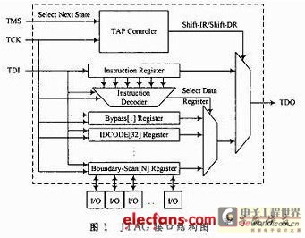
JTAG is a test standard proposed by the Joint Test Action Group of IEEE. This standard was originally used to solve the test problems caused by the increasing chip integration and board-level device density. Now this standard has been adopted by most device manufacturers and designed into chip circuits to support their device in-system debugging or programming functions. For the CPLD device used in this article, the structure of its JTAG interface is shown in Figure 1.

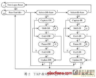
The JTAG standard defines four basic units: test access port TAP (Test Access Port), data register, instruction register and TAP controller. The TAP port contains four JTAG signals: test clock input pin TCK, test data input pin TDI, test data output pin TDO and test mode selection pin TMS. The data register mainly includes two types: BYPASS register and BSR (Botlndary Scan Register) register. BSR is composed of BSC (Botmdary Scan Cell) in series. It is through the BSC scan chain circuit that the CPLD configuration information from TDI can be moved into the chip, thereby realizing the erase and programming functions of the device. The TAP controller is actually a state machine containing 16 states, which controls the test access port, instruction register and data register. The TAP controller state transition diagram is shown in Figure 2.
The state of the TAP controller is controlled by the TMS and TCK signals. When the data on TDI needs to be moved to the instruction register, the TAP controller can enter the Shift-IR state; when the data on TDI needs to be moved to the data register, it can enter the Shift-DR state. Through the state transition of the TAP controller, the configuration information of the CPLD can be moved into its internal logic.
In the PC-based programming method, the configuration information file of the CPLD is stored in the PC. The download software running in the PC continuously reads the configuration information of the device and simulates the timing and logic of the JTAG test port through its parallel interface to achieve its software update and download. This article will use the DSP in the navigation computer system to implement this programming method: the CPLD configuration file is sent to the navigation computer system through the DSP's UART serial port, and then the DSP parses and executes the instructions in the configuration file, and simulates the JTAG port signal behavior through the DSP's I/O port to achieve the function of updating the CPLD device software. Based on this solution, it is possible to use an ordinary serial port to conveniently perform remote programming and updating of the CPLD.
 In order to realize the serial software update solution of CPLD device based on DSP in the navigation computer system proposed in this paper, the following three problems need to be solved in hardware:
(1) The DSP used in the navigation computer system must have at least four free I/O ports, which are used to simulate the four JTAG signal timing signals of the CPLD.
(2) The navigation computer system must include a UART communication interface to receive the CPLD configuration file. This UART interface cannot be controlled by the CPLD to avoid the problem that the UART communication port is no longer available after a CPLD programming failure.
(3) The navigation computer system should ensure sufficient storage space for the CPLD configuration information files.
The DSP used in this paper is the TMS320C6713B chip from TI, which supports 16 general-purpose input and output ports (GPIO). In this navigation computer system, 12 GPIO ports are already occupied, and the remaining 4 GPIO ports can be used to connect the 4 JTAG signal pins of the CPLD.
TMS320C6713B itself does not support the UART communication interface. Its on-chip peripherals include two multi-channel buffered serial interfaces (McBSP). The McBSP interface supports full-duplex serial communication, but the data transmission and reception requires independent frame synchronization signals. According to the application technology report provided by TI, the McBSP interface can support the UART communication standard after the software or hardware is modified and designed. The software modification method is to simulate the UART timing by configuring the McBSP interface as a general I/O interface; the hardware modification method is to configure the McBSP interface in serial port mode. The frame synchronization signal FSR received in the McBSP interface comes from the UART's transmit data line Tx. When the falling edge of Tx is detected, the McBSP starts sampling and receiving data internally. After that, the falling edge of Tx will be ignored until the start bit of the next byte triggers the internal frame to receive new data again; the frame synchronization signal FSR is generated by the McBSP circuit when the UART data start bit is sent. This paper uses hardware modification and oversampling software measures to design a multi-channel buffered serial interface McBSP0 into an interface that supports the UART communication standard.
The CPLD configuration information file used in this navigation computer system is in serial vector format (SVF), which can be generated on the Xilinx software development platform ISE. SVF is a specification used to describe the operation of the IEEE1149.1 (JTAG) bus. It contains the instructions and data required for programming and describes the scanning operation process and behavior between the states in the TAP test access port state diagram. Since the SVF file is in ASCII format, it occupies a large storage space. It can be converted into a more concise and compact binary format: XSVF file. For the CPLD device used in this system, when only programming operations are performed on it, the XSVF file size is 129720B. After erasing and verifying operations, the XSVF file size is 259533B. Based on the above analysis, the hardware circuit structure of the embedded navigation computer system designed in this paper for updating the CPLD device in the system software through the UART interface is shown in Figure 3.

In Figure 3, the UART communication port is implemented by the multi-channel buffered serial port McBSP0 on the DSP chip. In order to store the XSVF file containing the CPLD configuration information received through the UART port, this system has expanded a 512kB SRAM. The FLASH chip is used to store the navigation computer system upgrade firmware and application programs. The JTAG port of the CPLD is directly connected to the 4 idle GPIO ports of the DSP. In order to improve the flexibility of CPLD device programming, the CPLD program download interface connected to the PC parallel port is retained in this system. On the basis of hardware design, in order to realize the software update of the CPLD by simulating the JTAG signal timing logic through the DSP's GPIO port, it is necessary to strictly follow the port signal timing requirements in the JTAG standard. For the CPLD device used in this article, the JTAG port signal timing relationship is shown in Figure 4.

As shown in Figure 4, the following three items need to be considered for the JTAG port timing logic:
(1) The JTAG interface requires a minimum clock cycle TCKMIN.
(2) The JTAG interface samples the TMS and TDI signals on the rising edge of TCK. Therefore, before the rising edge of TCK, TMS and TDI must have a minimum setup time of TMSS and TDIS, respectively, and after the falling edge of TCK, they must be maintained for a minimum time of TMSH and TDIH, respectively.
(3) At the falling edge of TCK, the JTAT interface outputs a new TDO value and maintains it for at least TDOV.
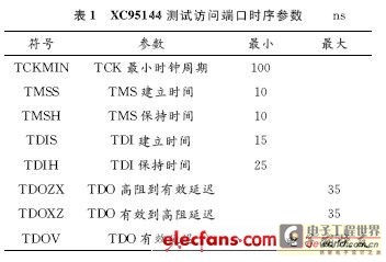
The JTAG port timing parameter requirements of the CPLD used in this article are shown in Table 1.

In the navigation computer system designed in this paper, the working frequency of DSP is 200MHz. Using the library function provided by TI, the maximum clock frequency simulated by the GPIO port of the DSP does not exceed 3MHz, which can meet the maximum 10MHz requirement corresponding to the TCKMIN parameter in the table. For parameter requirements such as setup and hold time, they can be achieved through software delay or timer. Since in the application of this system, DSP focuses on the software update of CPLD during power-on, this paper will use software delay to achieve these parameter requirements. The designed JTAG port signal level driver function module code is as follows:

Using the above code, the simulated JTAG clock signal frequency is 367.6kHz.
When configuring the CPLD device, the DSP continuously reads instructions and parameters from the XSVF file stored in the SRAM, and performs corresponding operations according to different instructions. According to the functional characteristics, the instructions in the XSVF file mainly include four types of instructions: state transfer, instruction shift-in, data shift-in or shift-out, and idle wait. The state transfer instruction is used to control the TAP state machine to enter the state corresponding to the next XSVF instruction operation. In the XSVF file, each state in Figure 2 corresponds to a byte of encoding; the instruction shift-in is used to shift the instruction code on TDI into the corresponding instruction register; the data shift-in or shift-out instruction can shift the data on TDI into the internal logic of the CPLD device, and can capture the data shifted out from TDO; the idle wait instruction can provide the time required to wait for the internal logic to respond successfully after shifting in the CPLD erase instruction or data.
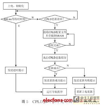
Based on the above design, the CPLD update process designed in serial mode is shown in Figure 5.

In Figure 5, the system first receives the programming configuration file of the CPLD through the serial port of the DSP. After receiving the configuration file, the CPLD software update can be completed within 35 seconds. In practical applications, the update scheme in this article can quickly realize different system configuration schemes according to needs, such as the combination of INS and GPS. Or the combination with geomagnetism, etc., without changing the hardware again, it can be used with a variety of sensors, overcoming the disadvantages of software update through common PCs and download cables, avoiding a series of tedious work such as repeated opening and assembly of the system, improving the efficiency of on-site debugging, and thus improving the adaptability of the navigation computer system.
4 Conclusion
Through hardware and software design, this paper realizes the serial method of software update of CPLD device based on DSP. At present, it has been successfully applied in the embedded navigation computer system based on DSP and CPLD developed by our research group. Compared with the commonly used programming method based on PC parallel port, this serial port update method solves the problem that the download cable from parallel port to JTAG port is too long to reliably update CPLD. At the same time, it can realize the remote update of CPLD device in the system, avoid the disadvantages of tedious on-site removal of board for software update and upgrade, and improve the maintainability of the system. In addition, by adding an external network interface, the software update solution designed in this paper can also realize the remote update of CPLD device. The design of this paper has good applicability for the update and upgrade of embedded navigation computer system, improves the flexibility of system application, can be applied to a variety of navigation systems with different configurations, and can also adapt to different sensors and interfaces in a navigation computer system through different configurations of CPLD.
Previous article:Internal FLASH self-test method based on TMSF240 chip
Next article:CAN bus data acquisition system solution based on DSPIC30F3013
- Popular Resources
- Popular amplifiers
- Analysis of the application of several common contact parts in high-voltage connectors of new energy vehicles
- Wiring harness durability test and contact voltage drop test method
- Sn-doped CuO nanostructure-based ethanol gas sensor for real-time drunk driving detection in vehicles
- Design considerations for automotive battery wiring harness
- Do you know all the various motors commonly used in automotive electronics?
- What are the functions of the Internet of Vehicles? What are the uses and benefits of the Internet of Vehicles?
- Power Inverter - A critical safety system for electric vehicles
- Analysis of the information security mechanism of AUTOSAR, the automotive embedded software framework
- Brief Analysis of Automotive Ethernet Test Content and Test Methods
 Professor at Beihang University, dedicated to promoting microcontrollers and embedded systems for over 20 years.
- LED chemical incompatibility test to see which chemicals LEDs can be used with
- Application of ARM9 hardware coprocessor on WinCE embedded motherboard
- What are the key points for selecting rotor flowmeter?
- LM317 high power charger circuit
- A brief analysis of Embest's application and development of embedded medical devices
- Single-phase RC protection circuit
- stm32 PVD programmable voltage monitor
- Introduction and measurement of edge trigger and level trigger of 51 single chip microcomputer
- Improved design of Linux system software shell protection technology
- What to do if the ABB robot protection device stops
- Learn ARM development(15)
- Analysis of the application of several common contact parts in high-voltage connectors of new energy vehicles
- Wiring harness durability test and contact voltage drop test method
- From probes to power supplies, Tektronix is leading the way in comprehensive innovation in power electronics testing
- From probes to power supplies, Tektronix is leading the way in comprehensive innovation in power electronics testing
- Sn-doped CuO nanostructure-based ethanol gas sensor for real-time drunk driving detection in vehicles
- Design considerations for automotive battery wiring harness
- Do you know all the various motors commonly used in automotive electronics?
- What are the functions of the Internet of Vehicles? What are the uses and benefits of the Internet of Vehicles?
- Power Inverter - A critical safety system for electric vehicles
- Battery voltage detection simulation + program based on MSP430
- [Nucleo G071 Review] I2C OLED&AD Collection
- The Three Realms of Oscilloscopes.pdf
- Summary of DSP 28377 online upgrade examples
- About MSP430F5438A upgrade failure
- Yesterday there was a strong wind and heavy rain, but today there is no wind or rain and no clear sky
- FPGA Implementation of ECT Image Reconstruction Algorithm
- Designing Current Loops Using the MSP430 MCU Smart Analog Combo
- The difference between HISPI and MIPI protocols.
- Can the analog watchdog of stm32f103ve be used for power-off detection?

 AZ358CMTR-E1


 京公网安备 11010802033920号