The AD10242 circuit is a high-speed analog-to-digital converter (ADC) launched by the American ADI Company. With a sampling speed of up to 40MHz per second, it is the latest high-speed, high-performance, low-power 12-bit dual-channel analog-to-digital converter. It is powered by ±5.0V power supply, and its input signal can be either bipolar or unipolar. On-chip tracking/protection amplifier (T/H), reference power supply and output buffer. The two channels in the chip are completely independent, each with its own decoding and analog input. Each channel uses laser correction gain and offset matching to ensure that the crosstalk between the two channels is better than 80dB. This circuit is undoubtedly an ideal choice for small-sized, high-speed, highly integrated embedded processing systems.
1 AD10242 core introduction
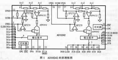
Each channel in the AD10242 integrates three monolithic devices, AD9632, OP279, and AD9042, as well as multiple resistors and decoupling capacitors. The internal structure of AD10242 is shown in Figure 1. Its core device is the AD9042. The input signal can be selected from ±0.5V, ±1.0V, and ±2.0V through a precision resistor divider. The resistor divider method can be used to protect the internal amplifier AD9632 from providing a 0.4V input voltage. The AD9632 is a DC-coupled horizontal phase shift circuit provided to the AD9042 analog-to-digital converter. The amplifier is configured in a non-invertible mode, where the AC signal is modified to provide a constant input to the ADC, centered around the AD9042's internal reference voltage. AD10242 can be used in signal processing application systems such as radar signal processing, communication receivers, FILR signal processing, and secure communications.

The core device AD9042 in the AD10242 is based on AD's high-speed complementary bipolar processing technology and adopts an improved multi-channel parallel structure design to ensure a distortion-free dynamic range of 80dB on a 20MHz bandwidth, with a typical signal-to-noise ratio of 68dB. . The AD9042 analog-to-digital converter adopts a two-level conversion mode. This design can ensure 12-bit accuracy at lower power without using laser correction. Its 1V (peak-to-peak) single-ended analog input and 2.4V midpoint voltage form a single-ended input differential output amplifier A1 and two input signals. The A1 output can be used to drive the first tracking/protection amplifier (TH1), and a high state on the encoding input can place TH1 in a hold state. The hold signal of TH1 is used to generate the input of a 6-bit coarse conversion ADC value. The 6-bit fine conversion value data can drive a 6-bit DAC, and the 6-bit coarse conversion can be simulated by the TH2 input at the input end of TH3. The values are subtracted to generate a residual difference signal, which is amplified by the difference amplifier A2 through the hold amplifier (TH3) in the next clock cycle, and then converted by the 7-bit precision conversion ADC to generate a 7-bit data code, one of which Code overlap is used to adjust the first 6-bit ADC generation. The 6-bit fine conversion code and the 7-bit fine conversion code are combined and corrected in the digital error correction logic to produce the output code (12-bit parallel data), which is output in two's complement format in a CMOS-compatible mode.
2 Pin functions of AD10242
3 Application of AD10242
3.1 Signal input of AD10242

The analog input of the AD10242 can be designed as a DC-coupled bipolar input (±0.5V, ±1.0V, ±2.0V), or it can be configured as a unipolar input through an external resistor. Connect a 2.43kΩ variable resistor between UPOS and UCOM (can be used for offset calibration) to achieve positive input of 1V, 2V, 4V. Connect a 2.43kΩ variable resistor between UNEG and UCOM to achieve - 1V, -2V, -4V negative input.
3.2 Coding signal input of AD10242
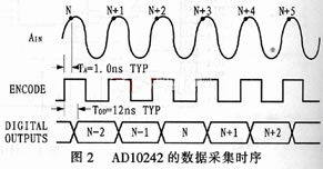
The logic interface of AD10242 is compatible with TTL and CMOS logic. It relies on the beat of the encoded signal ENCODE to collect data on its rising edge. The signal source driving the ENCODE pin must be clean and non-oscillating, because the oscillating signal source will reduce the SNR index. , the timing is shown in Figure 2.
The encoded signal input terminal of AD10242 can be connected to the differential input stage. When ENCODE or other input signals are not connected, the input stage bias voltage is 1.6V. For TTL or CMOS applications, the code signal source should be connected to ENCODE. ENCODE can be connected to ground through a low value inductor or high frequency chip capacitor.

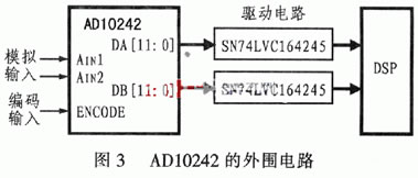
Figure 3 shows the circuit diagram of the interface connection between AD10242 and DSP.
3.3 Power supply
Since the AD10242 uses an analog ±5V power supply and a digital ±5V power supply, it is best to feed them separately during design, because fast digital oscillation may couple conversion noise back to the analog power supply. Each power supply pin must be connected to a 10μF tantalum capacitor and a 0.01μF chip state capacitor to decouple each power supply. The decoupling components should be as close as possible to the A/D converter. The decoupling of the analog power supply must be connected to the analog ground point first, and the decoupling of the digital power supply must be connected to the digital ground point first. The interconnection between analog ground and digital ground can only occur at the power common terminal.
4 Hardware interface with DSP
The basic simulation of real-time signal processing system generally adopts the "ADC+CPU (DSP, ARM, etc.) + DAC" structure. The design is generally to first convert it into a digital signal through the ADC subsystem, and then use the CPU subsystem to The digital signal is processed, and then the processed digital signal is converted back into an analog signal through the D/A converter subsystem. This system is a traditional real-time signal processing system based on DSP. This system uses AD10242 as the ADC acquisition module, which can ensure the system's 10-bit accuracy, 28MHz sampling speed, 2-channel parallel acquisition and ±2.0V analog input requirements. Since the DSP uses TI's TMS320C6701 high-performance floating-point processor, its core voltage is 1.8V and the peripheral I/O voltage is 3.3V. Therefore, a driver circuit must be added after the ADC. This design uses the SN74LVC164245 driver.
Previous article:New D/A converter AD9755 and its application
Next article:AD10242 dual-channel high-speed ADC and its application
Recommended ReadingLatest update time:2024-11-16 17:44


- Popular Resources
- Popular amplifiers
-
 Operational Amplifier Practical Reference Handbook (Edited by Liu Changsheng, Zhao Mingying, Liu Xu, etc.)
 -
 A Complete Illustrated Guide to Operational Amplifier Applications (Written by Wang Zhenhong)
 -
 Design of isolated error amplifier chip for switching power supply_Zhang Rui
 -
 DAM medium wave transmitter high frequency power amplifier module test platform_Tian Tian
- High signal-to-noise ratio MEMS microphone drives artificial intelligence interaction
- Advantages of using a differential-to-single-ended RF amplifier in a transmit signal chain design
- ON Semiconductor CEO Appears at Munich Electronica Show and Launches Treo Platform
- ON Semiconductor Launches Industry-Leading Analog and Mixed-Signal Platform
- Analog Devices ADAQ7767-1 μModule DAQ Solution for Rapid Development of Precision Data Acquisition Systems Now Available at Mouser
- Domestic high-precision, high-speed ADC chips are on the rise
- Microcontrollers that combine Hi-Fi, intelligence and USB multi-channel features – ushering in a new era of digital audio
- Using capacitive PGA, Naxin Micro launches high-precision multi-channel 24/16-bit Δ-Σ ADC
- Fully Differential Amplifier Provides High Voltage, Low Noise Signals for Precision Data Acquisition Signal Chain
- Innolux's intelligent steer-by-wire solution makes cars smarter and safer
- 8051 MCU - Parity Check
- How to efficiently balance the sensitivity of tactile sensing interfaces
- What should I do if the servo motor shakes? What causes the servo motor to shake quickly?
- 【Brushless Motor】Analysis of three-phase BLDC motor and sharing of two popular development boards
- Midea Industrial Technology's subsidiaries Clou Electronics and Hekang New Energy jointly appeared at the Munich Battery Energy Storage Exhibition and Solar Energy Exhibition
- Guoxin Sichen | Application of ferroelectric memory PB85RS2MC in power battery management, with a capacity of 2M
- Analysis of common faults of frequency converter
- In a head-on competition with Qualcomm, what kind of cockpit products has Intel come up with?
- Dalian Rongke's all-vanadium liquid flow battery energy storage equipment industrialization project has entered the sprint stage before production
- Allegro MicroSystems Introduces Advanced Magnetic and Inductive Position Sensing Solutions at Electronica 2024
- Car key in the left hand, liveness detection radar in the right hand, UWB is imperative for cars!
- After a decade of rapid development, domestic CIS has entered the market
- Aegis Dagger Battery + Thor EM-i Super Hybrid, Geely New Energy has thrown out two "king bombs"
- A brief discussion on functional safety - fault, error, and failure
- In the smart car 2.0 cycle, these core industry chains are facing major opportunities!
- The United States and Japan are developing new batteries. CATL faces challenges? How should China's new energy battery industry respond?
- Murata launches high-precision 6-axis inertial sensor for automobiles
- Ford patents pre-charge alarm to help save costs and respond to emergencies
- New real-time microcontroller system from Texas Instruments enables smarter processing in automotive and industrial applications
- Testing solutions for redundant link networks
- Key wireless technologies for 5G systems
- [NXP Rapid IoT Review] + Rapid IoT App Running Error
- How to Design an RF Power Amplifier: The Basics
- What is the principle of touch switch?
- What is jitter and phase noise?
- [Shanghai Hangxin ACM32F070 development board + touch function evaluation board evaluation] + OLED screen display driver
- Tailing Micro B91 Development Kit Burning Pitfalls Record
- Antai Testing - Sharing of Maintenance Experience of Tektronix AFG3021 Arbitrary Signal Generator
- Interrupt vectors for ARM (Cortex-M3)

 Operational Amplifier Practical Reference Handbook (Edited by Liu Changsheng, Zhao Mingying, Liu Xu, etc.)


 京公网安备 11010802033920号