As a new high-tech storage product in the information age, IC smart cards have the advantages of large capacity, strong confidentiality and easy portability, and are widely used in various fields of social life. The so-called IC card is made by embedding an IC chip containing a non-volatile storage unit NVM or an integrated microcontroller MCU in a plastic substrate, which mainly includes three parts: a plastic substrate (with or without a magnetic stripe), a contact surface, and an IC chip. The traditional IC card production process is: thinning and dicing the silicon wafer after testing and information writing, separating it into small chips, and then making an IC card module through processes such as chip loading, wire bonding, and encapsulation, and finally embedding it into an IC card plastic substrate.
With the improvement of IC product manufacturing technology and the emergence of high-performance LSI, IC smart cards are constantly developing in the direction of diversified functions and intelligence to meet people's pursuit of convenience and speed. However, many failure problems such as password verification errors, data loss, data writing errors, garbled characters, all "0" and all "F" that occur during use have seriously affected the widespread application of IC cards. Therefore, it is necessary to analyze the failed IC cards in combination with the manufacturing process and use environment of IC cards, conduct in-depth research on their failure modes and failure mechanisms, and explore the root causes of failures so as to take corresponding measures to improve the quality and performance of IC cards1.
From the analysis of failed IC card samples, it is found that chip fragmentation, internal lead shedding (desoldering, cold soldering, etc.), chip circuit breakdown and other phenomena are the main causes of IC card failure. This article focuses on the research and discussion of IC card chip fragmentation, bonding failure mode and mechanism, and briefly introduces other failure modes.
1 Failure caused by chip fragmentation
Since IC cards use thin/ultra-thin chips, chip fragmentation is the main cause of their failure, accounting for more than half of the total number of failures, mainly manifested as IC card data writing errors, garbled codes, all "0" and all "F".
Electrical tests were conducted on 1739 failed IC cards provided by different companies. 100 samples with failure modes of all "0" and all "F" were selected for corrosion and opening of the front and back sides of the IC cards. Optical microscope (OM) observations showed that most of the cracks were in the shape of "X" or "T", and some were single cracks that penetrated the chip and were slightly bent at the point of action of the ejector pin, as shown in Figure 1. More than 50% of the cracks in the broken chips were located near the center of the chip and perpendicular to the edge; the cracks in the remaining chips were close to the edge of the chip or concentrated on the chip.

Figure 2 OM photo of chip back grinding damage
1.1 Silicon wafer thinning
The standard silicon wafer back thinning process includes three steps: wafer bonding, grinding (coarse grinding, fine grinding), and etching. The commonly used mechanical grinding method will inevitably cause damage to the surface and subsurface of the silicon wafer (Figure 2). The surface damage is divided into three layers: an amorphous layer with microcracks; a deeper lattice dislocation layer; and an elastic deformation layer. After coarse grinding and fine grinding, a thin layer with a depth of 15 to 20 μm and microdamage and microcracks remains on the back of the silicon wafer, which greatly affects the strength of the silicon wafer. Therefore, it is necessary to use the etching method to remove the residual lattice damage layer on the back of the silicon wafer to prevent the silicon wafer from breaking due to residual stress. The experiment found that the silicon wafer with an original thickness of 725 μm can obtain the maximum strength value of 3 when the etching depth is about 25 μm after grinding; at the same time, the analysis shows that the chip breaks during bonding and testing, which is often caused by the damage caused by grinding not being completely removed in the subsequent etching or chemical mechanical polishing.
Figure 6 Schematic diagram of ejector scratches
Figure 8 Bonding-related failures
Water vapor erosion can cause electrolytic effects, which greatly accelerate metal electromigration. Contamination of the pad substrate with impurities such as C will lead to the generation of voids, causing pad bulges. Figure 8(c) shows a failed sample with discontinuous electrical characteristics. SEM and EDX (Figure 9) analysis proves that there is a bursting phenomenon in the connection part and chlorine exists in the pad.
3 Injection molding-related failures
Like other plastic-encapsulated IC products, punching wires and voids in encapsulation materials during injection molding can also cause IC card failure problems6. Epoxy molding materials are in a molten state during injection molding and are viscous moving fluids. Therefore, they have a certain impact force. The impact force acts on the gold wire, causing the gold wire to deviate. In extreme cases, the gold wire is broken, which is the so-called punching wire.
An effective method to protect against ESD is to design a specific protection circuit. Figure 10 is an IC card chip ESD protection circuit 7 based on CMOS technology. The structure includes two parts: the main protection circuit and the clamping circuit. When ESD occurs, the clamping circuit is first turned on to clamp the voltage on the input gate to a voltage lower than the gate breakdown voltage. The series resistor in the middle plays a current limiting role, and more importantly, the voltage on the PAD can trigger the opening of the main protection circuit, so that the ESD energy is released through the main protection circuit.

Reference address:Study on the Failure Mechanism of IC Smart Card
With the improvement of IC product manufacturing technology and the emergence of high-performance LSI, IC smart cards are constantly developing in the direction of diversified functions and intelligence to meet people's pursuit of convenience and speed. However, many failure problems such as password verification errors, data loss, data writing errors, garbled characters, all "0" and all "F" that occur during use have seriously affected the widespread application of IC cards. Therefore, it is necessary to analyze the failed IC cards in combination with the manufacturing process and use environment of IC cards, conduct in-depth research on their failure modes and failure mechanisms, and explore the root causes of failures so as to take corresponding measures to improve the quality and performance of IC cards1.
From the analysis of failed IC card samples, it is found that chip fragmentation, internal lead shedding (desoldering, cold soldering, etc.), chip circuit breakdown and other phenomena are the main causes of IC card failure. This article focuses on the research and discussion of IC card chip fragmentation, bonding failure mode and mechanism, and briefly introduces other failure modes.
1 Failure caused by chip fragmentation
Since IC cards use thin/ultra-thin chips, chip fragmentation is the main cause of their failure, accounting for more than half of the total number of failures, mainly manifested as IC card data writing errors, garbled codes, all "0" and all "F".
Electrical tests were conducted on 1739 failed IC cards provided by different companies. 100 samples with failure modes of all "0" and all "F" were selected for corrosion and opening of the front and back sides of the IC cards. Optical microscope (OM) observations showed that most of the cracks were in the shape of "X" or "T", and some were single cracks that penetrated the chip and were slightly bent at the point of action of the ejector pin, as shown in Figure 1. More than 50% of the cracks in the broken chips were located near the center of the chip and perpendicular to the edge; the cracks in the remaining chips were close to the edge of the chip or concentrated on the chip.

Figure 1 OM photo of chip backside cracking
Based on the physical mechanism of chip breakage and combined with the IC card manufacturing process (including the back-end process of silicon wafers, module strip production, and IC card molding process), the root cause of the breakage of thin IC card chips is analyzed in depth.
Figure 2 OM photo of chip back grinding damage
1.1 Silicon wafer thinning
The standard silicon wafer back thinning process includes three steps: wafer bonding, grinding (coarse grinding, fine grinding), and etching. The commonly used mechanical grinding method will inevitably cause damage to the surface and subsurface of the silicon wafer (Figure 2). The surface damage is divided into three layers: an amorphous layer with microcracks; a deeper lattice dislocation layer; and an elastic deformation layer. After coarse grinding and fine grinding, a thin layer with a depth of 15 to 20 μm and microdamage and microcracks remains on the back of the silicon wafer, which greatly affects the strength of the silicon wafer. Therefore, it is necessary to use the etching method to remove the residual lattice damage layer on the back of the silicon wafer to prevent the silicon wafer from breaking due to residual stress. The experiment found that the silicon wafer with an original thickness of 725 μm can obtain the maximum strength value of 3 when the etching depth is about 25 μm after grinding; at the same time, the analysis shows that the chip breaks during bonding and testing, which is often caused by the damage caused by grinding not being completely removed in the subsequent etching or chemical mechanical polishing.
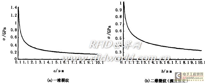
For a two-dimensional semi-elliptical crack with a fracture plane perpendicular to the chip surface, a depth of a and a length of 2b, Ccr=[(Φ2KIC2)/(1.2πσIC2)][2] is satisfied, where Ccr=(acrbcr)1/2, acr is the critical crack depth, bcr is the critical crack half length; crack geometry factor Φ=(1.2π)1/2/Y. Assuming the crack length is 2b and the depth is constant at 1μm, substituting the fracture toughness KIC=0.82MPa and Y=1.42, the critical strength of fracture under plane stress state and constant load conditions is σ=0.58/4b(GPa). The corresponding relationship between σ and the length and depth of the residual crack on the back of the chip is shown in Figure 3(b). It can be seen that the critical strength of chip fragmentation decreases sharply with the increase of microcrack length. When the crack is greater than 1μm, the downward trend gradually slows down and tends to a stable small value.
The grinding process will not only cause micro cracks on the back of the silicon wafer, but the residual stress on the surface will also cause the silicon wafer to warp. The back thinning process of the silicon wafer has a direct impact on chip fragmentation, so new technologies need to be developed to achieve back thinning process integration to improve the efficiency of silicon wafer thinning and reduce chip fragmentation.
The grinding process will not only cause micro cracks on the back of the silicon wafer, but the residual stress on the surface will also cause the silicon wafer to warp. The back thinning process of the silicon wafer has a direct impact on chip fragmentation, so new technologies need to be developed to achieve back thinning process integration to improve the efficiency of silicon wafer thinning and reduce chip fragmentation.

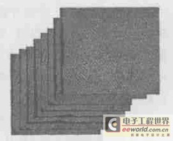
After thinning, the silicon wafer is sent to the dicing machine for dicing. The cross section of the dicing groove is often rough, usually with a small amount of microcracks and pits; in some places, the dicing is not cut to the bottom. When taking the wafer, the chip must be "forced" to separate by the force of the ejector pin, and the fracture is irregular. Figure 4 is an overlay of multiple samples. Experiments show that damage to the chip edge caused by dicing will also seriously affect the chip's fragmentation strength. For example, a chip with microcracks or grooves on the fracture will break under the instantaneous impact of the subsequent wire bonding process or the stress generated by the mismatch of the coefficient of thermal expansion (CTE) during the heat treatment after encapsulation, which causes the microcracks to expand.

In order to reduce the damage to the chip caused by the dicing process, new dicing technologies have been introduced: dicing before thinning (DBG) and dicing by thinning (DBT)5, that is, before thinning the back of the silicon wafer, a cut is made on the front by grinding or etching to achieve automatic separation of the chip after thinning. These two methods can effectively avoid/reduce the warping of the silicon wafer caused by thinning and the damage to the chip edge caused by dicing. In addition, the use of laser dicing technology with non-mechanical contact processing can also avoid micro cracks, fragments and other phenomena caused by mechanical dicing, greatly improving the yield rate.
1.3 Module process
The module process includes processes such as chip loading and encapsulation. During the chip loading process, the chip loading machine ejector pin lifts the chip from the chip film, and the vacuum suction head sucks the chip and bonds it to the lead frame of the chip card. If the process parameters of the chip mounter are not adjusted properly, the back of the chip will be damaged, seriously affecting the chip strength. For example, if the ejector force is uneven or too large, the ejector will pierce the blue film and directly act on the chip, leaving a circular damage pit on the back of the chip. Or the ejector has a certain amount of equal sliding process on the back of the chip, leaving a large scratch. This phenomenon accounts for a considerable proportion of broken chips.
Fig The action of the ejector pin can be equivalent to the pressure loading process of the Vicker indenter 4, which will cause local damage to the chip surface. Now the process of the ejector pin touching the back of the chip (not considering the slip of the ejector pin for the time being) is simplified to the ideal case of vertical loading on the spherically symmetrical plane. The change of the contact circle radius a between the two with the vertical load P is a=34PR(1-v2)/E+(1-v′2)/E′1/3=αP1/3, where R is the radius of the ejector pin end, E, v and E′, v′ are the Young's modulus and Poisson's ratio of the chip and the ejector pin end respectively. At the edge of the contact circle, the tensile stress component of the chip reaches the maximum value σm=12(1-2v)P0, where P0=P/πα2 is the vertical stress on the end, and σm is the stress acting in the radial direction and equal to the material surface. Since the tip radius of the ejector pin is small, v=0.28 for silicon material is taken. Under the action of 1N ejection force, the corresponding relationship between the maximum value of the chip tension component and the contact radius is shown in Figure 5. It can be seen that in the initial case, the contact radius is very small, and the initial value of the chip tension component can reach the GPa level. Compared with the previous calculation results, it can be seen that the ejection pin process is a major cause of chip fragmentation.
In addition, accompanied by the indentation effect, the chip often breaks into pieces, that is, some materials around the indentation are in the form of debris. When the ejection pin acts, transverse cracks will be generated in the deformation zone under the indentation surface. After the indentation effect disappears, the transverse cracks will proliferate until the sample surface, resulting in the generation of fragments. In general, the greater the pressure, the more serious the fragmentation phenomenon.
When the ejection pin acts on the back of the chip during the sliding process, the end of the ejection pin is subjected to the friction resistance proportional to the vertical load, which increases the tensile stress of the contact circle. At the same time, when the ejection pin slides over the chip, it will leave strip-shaped scratches on its back, which may produce fine debris and wedge into the silicon substrate material to form microcracks, greatly affecting the strength of the chip.
OM observation of the back of the unsealed IC card chip revealed that most of the broken chips had pin scratches at or near the cracks, most of which were straight lines with hooks, and the cracks were bent to varying degrees at the scratches. The scratches were large, generally tens of μm long, greater than 10 μm wide, and had a certain depth of about several μm (Figure 6 is a schematic diagram of the statistical data of the scratch shapes and sizes of 20 samples).
Under a specific contact radius, the tensile stress outside the contact circle on the chip surface and the radial distance from the contact center satisfy σr=σm(a/r)2, and σr decreases as the radial distance r from the contact center increases. Therefore, within a certain range from the pin point of action, there is still a tensile stress surface layer on the chip surface, which provides very favorable conditions for crack generation and expansion.
Figure 6 Schematic diagram of ejector scratches
In the IC card molding process, due to the manufacturing process factors, there are certain differences between the module thickness and the card base groove geometry, which cannot be completely matched, which will cause a greater multiple stress. In addition, the thermal expansion and contraction of different materials or external force distortion during use can also easily cause chip breakage.
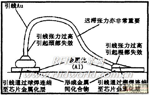
Figure 7 Failure mechanism in the bonding wire process

Figure 7 Failure mechanism in the bonding wire process
2 Bonding-related failures
In the IC card assembly process, failures caused by bonding are also one of the important factors affecting the quality and reliability of IC cards. Bonding failures are mainly manifested as discontinuities in the electrical characteristics of IC cards, such as open circuits accompanied by short circuits, leakage, etc., or "input high" or "input low" failures. Figure 7 shows many failure mechanisms related to bonding6.
In the IC card assembly process, failures caused by bonding are also one of the important factors affecting the quality and reliability of IC cards. Bonding failures are mainly manifested as discontinuities in the electrical characteristics of IC cards, such as open circuits accompanied by short circuits, leakage, etc., or "input high" or "input low" failures. Figure 7 shows many failure mechanisms related to bonding6.
Figure 8 Bonding-related failures
Water vapor erosion can cause electrolytic effects, which greatly accelerate metal electromigration. Contamination of the pad substrate with impurities such as C will lead to the generation of voids, causing pad bulges. Figure 8(c) shows a failed sample with discontinuous electrical characteristics. SEM and EDX (Figure 9) analysis proves that there is a bursting phenomenon in the connection part and chlorine exists in the pad.
3 Injection molding-related failures
Like other plastic-encapsulated IC products, punching wires and voids in encapsulation materials during injection molding can also cause IC card failure problems6. Epoxy molding materials are in a molten state during injection molding and are viscous moving fluids. Therefore, they have a certain impact force. The impact force acts on the gold wire, causing the gold wire to deviate. In extreme cases, the gold wire is broken, which is the so-called punching wire.
Assuming that the molten plastic encapsulation material is an ideal fluid and the thickness of the plastic encapsulation body is not considered, the impact of the plastic encapsulation material flow on the gold wire can be expressed as F=Kfηυsinθ, where F is the impact per unit area, Kf is a constant, η is the viscosity of the molten plastic encapsulation material, υ is the flow velocity, and θ is the angle between the flow direction and the gold wire. From the formula, it can be seen that the greater the viscosity of the plastic encapsulation material, the faster the flow velocity, and the larger the angle θ, the greater the impact force generated, and the more serious the wire punching, which will cause short circuits or lead wire connection detachment, resulting in IC card failure.
In addition, the bubbles, small holes and pits (porous surface) left in the injection molding process will diffuse and increase after subsequent processes, which is easy to cause moisture and other harmful impurities to invade, accelerate the formation of IMC, and cause pad corrosion.
4 Failure caused by electrostatic discharge
Electrostatic discharge (ESD) is the transmission of static charge between two objects with different electrostatic potentials caused by direct contact or electrostatic field induction, which often causes many failures such as current melting, charge injection, oxide layer damage and film burning in chip circuits.
An effective method to protect against ESD is to design a specific protection circuit. Figure 10 is an IC card chip ESD protection circuit 7 based on CMOS technology. The structure includes two parts: the main protection circuit and the clamping circuit. When ESD occurs, the clamping circuit is first turned on to clamp the voltage on the input gate to a voltage lower than the gate breakdown voltage. The series resistor in the middle plays a current limiting role, and more importantly, the voltage on the PAD can trigger the opening of the main protection circuit, so that the ESD energy is released through the main protection circuit.

In addition, the occurrence of ESD can be effectively reduced by improving the production process and controlling the use environment. Traditional IC cards use wire bonding strip technology, and chip fragmentation is its main failure mechanism. By improving the process technology of grinding and dicing, improving the process quality of assembly (especially the ejector process during chip installation), bonding, module inlay, etc., the chip fragmentation rate can be greatly reduced, and the yield and reliability of IC cards can be improved.
In addition, failures related to wire bonding and injection molding, such as cold soldering, desoldering, loose or tight wires, punching, or IMC formed due to the intrusion of external moisture and electrical factors, will reduce the reliability of IC cards and cause IC card failure. The occurrence of such failures can be reduced by improving the corresponding process technology. ESD is also one of the important mechanisms of IC card failure. In severe cases, it will cause Al wire/polysilicon resistor burnout, transistor gate oxide layer damage or junction damage. For this, the IC card chip's ability to resist ESD can be improved by designing a special ESD protection circuit to improve the reliability of the IC card.
In addition, failures related to wire bonding and injection molding, such as cold soldering, desoldering, loose or tight wires, punching, or IMC formed due to the intrusion of external moisture and electrical factors, will reduce the reliability of IC cards and cause IC card failure. The occurrence of such failures can be reduced by improving the corresponding process technology. ESD is also one of the important mechanisms of IC card failure. In severe cases, it will cause Al wire/polysilicon resistor burnout, transistor gate oxide layer damage or junction damage. For this, the IC card chip's ability to resist ESD can be improved by designing a special ESD protection circuit to improve the reliability of the IC card.
Previous article:The technology of tap water flow monitoring terminal designed by GPRS
Next article:Thermal Far Infrared Ceramic Conductive Glaze Thermal Resistor
- Popular Resources
- Popular amplifiers
Latest Analog Electronics Articles
- High signal-to-noise ratio MEMS microphone drives artificial intelligence interaction
- Advantages of using a differential-to-single-ended RF amplifier in a transmit signal chain design
- ON Semiconductor CEO Appears at Munich Electronica Show and Launches Treo Platform
- ON Semiconductor Launches Industry-Leading Analog and Mixed-Signal Platform
- Analog Devices ADAQ7767-1 μModule DAQ Solution for Rapid Development of Precision Data Acquisition Systems Now Available at Mouser
- Domestic high-precision, high-speed ADC chips are on the rise
- Microcontrollers that combine Hi-Fi, intelligence and USB multi-channel features – ushering in a new era of digital audio
- Using capacitive PGA, Naxin Micro launches high-precision multi-channel 24/16-bit Δ-Σ ADC
- Fully Differential Amplifier Provides High Voltage, Low Noise Signals for Precision Data Acquisition Signal Chain
MoreSelected Circuit Diagrams
MorePopular Articles
- Innolux's intelligent steer-by-wire solution makes cars smarter and safer
- 8051 MCU - Parity Check
- How to efficiently balance the sensitivity of tactile sensing interfaces
- What should I do if the servo motor shakes? What causes the servo motor to shake quickly?
- 【Brushless Motor】Analysis of three-phase BLDC motor and sharing of two popular development boards
- Midea Industrial Technology's subsidiaries Clou Electronics and Hekang New Energy jointly appeared at the Munich Battery Energy Storage Exhibition and Solar Energy Exhibition
- Guoxin Sichen | Application of ferroelectric memory PB85RS2MC in power battery management, with a capacity of 2M
- Analysis of common faults of frequency converter
- In a head-on competition with Qualcomm, what kind of cockpit products has Intel come up with?
- Dalian Rongke's all-vanadium liquid flow battery energy storage equipment industrialization project has entered the sprint stage before production
MoreDaily News
- Allegro MicroSystems Introduces Advanced Magnetic and Inductive Position Sensing Solutions at Electronica 2024
- Car key in the left hand, liveness detection radar in the right hand, UWB is imperative for cars!
- After a decade of rapid development, domestic CIS has entered the market
- Aegis Dagger Battery + Thor EM-i Super Hybrid, Geely New Energy has thrown out two "king bombs"
- A brief discussion on functional safety - fault, error, and failure
- In the smart car 2.0 cycle, these core industry chains are facing major opportunities!
- The United States and Japan are developing new batteries. CATL faces challenges? How should China's new energy battery industry respond?
- Murata launches high-precision 6-axis inertial sensor for automobiles
- Ford patents pre-charge alarm to help save costs and respond to emergencies
- New real-time microcontroller system from Texas Instruments enables smarter processing in automotive and industrial applications
Guess you like
- C2000GPRS connection failure
- An Active Filter Experiment
- Must-see! Illustrated guide to the Internet of Things
- Please help! The ADC sampling fluctuation in stm32h743 is very large, and the 16-bit resolution exceeds the 8-bit fluctuation
- Apply for ufun learning board, introductory & deep learning simulation, engineering skills
- I downloaded a source code from the Internet. Please help me find out what IDE this project was developed in. Thanks
- X-NUCLEO-IKS01A3 MakeCode Driver (Extension) Collection
- This strange circuit
- EEWORLD University ---- test
- What is ModBus? What are the differences and connections with RS485 protocol?

 AD744TH/883B


 京公网安备 11010802033920号