1 Common modulation methods for transmitters
There are two common transmitter modulation methods: intermediate frequency modulation and RF direct modulation. Intermediate frequency modulation is to modulate at a lower intermediate frequency, and then move the intermediate frequency signal to the required transmission carrier frequency through frequency conversion such as mixing. Direct RF modulation is performed at the RF frequency to be transmitted, and the baseband signal is directly modulated to the RF carrier frequency without a frequency conversion link. The two modulation methods have their own advantages and disadvantages. The main comparison is shown in Table 1.

Since IF modulation is generally performed at a lower frequency, the modulator has a wide range of choices and is easy to implement. In addition, due to the existence of the frequency conversion link, the DC component of the modulation and the carrier leakage are well suppressed. However, due to the use of the frequency conversion link, compared with direct RF modulation, it is necessary to add a mixer, a filter and a first-level local oscillator, which increases the system complexity, increases the system cost, and reduces reliability. At the same time, due to the low IF frequency, it is difficult to achieve a higher modulation bandwidth.
The RF direct modulation method has the advantages of simple and reliable system, wide modulation bandwidth, few components, low cost, etc., and is more suitable for applications with high data rate and small size. However, it has problems such as limited adaptability to carrier frequency, large carrier leakage, and high requirements for local oscillator. It is difficult to meet the index requirements when the requirements for carrier leakage and out-of-band attenuation are strict.
2 Transmitter Design
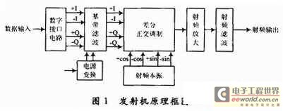
This system works in the S band dedicated to telemetry. Generally, the number of users is limited, and the requirements for carrier leakage and out-of-band attenuation are not very strict. However, the key problem of this system is that the available space in the telemetry cabin is small and it needs to resist strong overload of artillery shells. Therefore, this scheme uses RF direct modulation. The local oscillator and I, Q signals of this transmitter are all output in differential mode, and the modulation is realized by the modulator of the differential interface, which better suppresses the common mode interference in the circuit. Figure 1 is the principle block diagram of the transmitter. The baseband signal modulates the RF local oscillator through filtering, and then is output through RF amplification and low-pass filter to remove harmonics.

2.1 Digital Interface Design
Because the front-end digital circuit can directly output differential I, Q digital signals, the digital interface circuit was not designed in the transmitter at the beginning of the design. The differential I, Q signals output by the front-end digital circuit directly modulate the RF local oscillator. However, after actual tests, the modulation characteristics are too poor. The main reason is that the digital circuit output is difficult to match the modulator. Therefore, it was improved and an interface circuit composed of AD9761 dual differential output DAC was added to the transmitter. The circuit has a 40 MSPS conversion rate (single-channel 40 MSPS), 10 bit DAC, dual differential conversion output, and
It also has a 2x sampling interpolation filter function. The output of this circuit is current mode, which can achieve a good match with the modulator.
2.2 Baseband filter circuit design
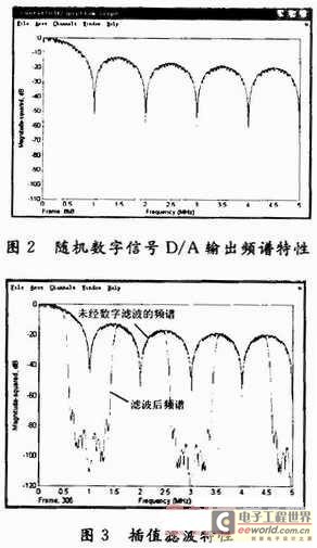
The spectrum of a random sequence with a symbol rate of 1 MHz is shown in Figure 2. Filtering the signal can suppress the sideband signal and reduce the bandwidth occupancy. If analog filtering is used, the filter order required is very high, which will increase the size of the filter and reduce the stability of the environment. The use of digital filtering technology can easily achieve high-order filtering, suppress the near-end out-of-band signal, and reduce the requirements for analog filters. The digital interface circuit used in this scheme is a low-pass interpolation filter circuit with a 43-order FIR with 2 times sampling, which is equivalent to adding a filter. The stopband suppression reaches 62 dB, so the spectrum characteristics of the modulated output signal are greatly improved, and the near-end spectrum outside the passband is greatly suppressed. For frequencies higher than the conversion clock, the filtering characteristics are periodically folded. Figure 3 shows the comparison between the spectrum after interpolation digital filtering and the original spectrum. The stopband suppression of the digital interpolation filter circuit enables the analog filter to have a wider transition band, and the circuit requirements are reduced.
To simplify the circuit, this solution uses a simpler RC filter circuit with a sidelobe suppression of 40 dB.

2.3 Local Oscillator Design
The local oscillator circuit generates the RF local oscillator signal. Since the orthogonal phase modulation has high performance requirements for the local oscillator signal, and direct RF modulation is used in this system, in order to achieve a certain carrier leakage control, a local oscillator circuit with differential output should be selected. This solution uses the ADF4360-1 integrated phase-locked loop (PLL) circuit to generate the RF local oscillator. ADF4360-1 is a complete phase-locked loop chip with integrated VCO from AD, which has the characteristics of small size, easy use, and reliable performance. The package is only 4 mm×4 mm, and can output RF signals of 2 050~2 450 MHz, and is controlled by a 3-wire serial interface.
2.4 Modulation Circuit
The modulation circuit mainly completes the direct RF modulation function. It uses a filtered dual-path differential modulation signal to modulate the RF local oscillator. This design selects the AD8346 orthogonal modulator produced by AD, which is a wide-band orthogonal modulator with an operating frequency range of 800 to 2 500 MHz. It has the characteristics of high modulation accuracy and low noise level. Its phase error is 1°, I, Q amplitude imbalance is 0.2 dB, and the noise level is -147 dBm/Hz. The frequency used in this project is 2.2 to 2.3 GHz. Through reasonable circuit layout and port matching, a good modulation effect is achieved, and the measured vector modulation error is 2% to 3%.
2.5 Amplifier Circuit
Since the signal amplitude after RF modulation is small, it must be effectively amplified to achieve the required power. In this scheme, a two-stage RF amplifier is used. The first stage uses HMC47 8MP86, and the second stage uses HMC457QS16G. The input and output of the two-stage amplifier are 50 Ω matched. The HMC478 has high gain, low noise figure and good linearity; the HMC457 has high output power, and its 1 dB compression output can reach 30.5 dBm. The gain of the two-stage amplifier is 41 dB in total. After deducting the loss of inter-stage matching, the final output is 29 dBm. Both amplifiers are industrial-grade products of Hittite, which can meet the temperature environment of -40 to +85°C, and both are surface-mounted packaging with strong impact and vibration resistance.
2.6 RF filter circuit design
The RF amplifier circuit inevitably has a certain degree of nonlinearity, which will produce harmonics of the operating frequency. In order to reduce out-of-band radiation and reduce interference to other systems, a microstrip low-pass filter circuit is designed to suppress the harmonics.
2.7 Power Supply Design
The power supply circuit is used to convert the 12 V unregulated input into 5 V and 3.3 V voltages used by various components of the transmitter. The 5 V is used to power the interface circuit and the amplifier circuit. Due to its high power consumption, a DC/DC conversion circuit is selected to achieve a higher conversion efficiency; the 3.3 V is used for the phase-locked local oscillator circuit, which is obtained by stepping down the 5 V using a linear voltage regulator circuit to reduce ripple. LT's LT3431 and LT1962 are used in the design. In order to reduce the power ripple during the printed circuit board wiring, the power supply wiring is optimized in detail.
3 Design Results
This project completed the circuit design on a φ75 mm circuit board, and the inter-stage matching adjustment was performed after assembly. The final indicators achieved were: local oscillator phase noise of -95dBc/Hz@1 kHz; local oscillator spurious suppression of 72 dBc; output signal power of 29 dBm; output signal EVM of 5.5%.
4 Conclusion
The transmitter has been developed and has passed environmental tests such as high and low temperature, shock, and vibration, and participated in a live-fire test of a low-altitude telemetry system. During the entire process, the transmitter worked stably and reliably and was able to achieve the design goals.
Previous article:Communication design of video intercom access control system
Next article:Design of identity code transmitter based on RFID technology
- Popular Resources
- Popular amplifiers
- High signal-to-noise ratio MEMS microphone drives artificial intelligence interaction
- Advantages of using a differential-to-single-ended RF amplifier in a transmit signal chain design
- ON Semiconductor CEO Appears at Munich Electronica Show and Launches Treo Platform
- ON Semiconductor Launches Industry-Leading Analog and Mixed-Signal Platform
- Analog Devices ADAQ7767-1 μModule DAQ Solution for Rapid Development of Precision Data Acquisition Systems Now Available at Mouser
- Domestic high-precision, high-speed ADC chips are on the rise
- Microcontrollers that combine Hi-Fi, intelligence and USB multi-channel features – ushering in a new era of digital audio
- Using capacitive PGA, Naxin Micro launches high-precision multi-channel 24/16-bit Δ-Σ ADC
- Fully Differential Amplifier Provides High Voltage, Low Noise Signals for Precision Data Acquisition Signal Chain
- Innolux's intelligent steer-by-wire solution makes cars smarter and safer
- 8051 MCU - Parity Check
- How to efficiently balance the sensitivity of tactile sensing interfaces
- What should I do if the servo motor shakes? What causes the servo motor to shake quickly?
- 【Brushless Motor】Analysis of three-phase BLDC motor and sharing of two popular development boards
- Midea Industrial Technology's subsidiaries Clou Electronics and Hekang New Energy jointly appeared at the Munich Battery Energy Storage Exhibition and Solar Energy Exhibition
- Guoxin Sichen | Application of ferroelectric memory PB85RS2MC in power battery management, with a capacity of 2M
- Analysis of common faults of frequency converter
- In a head-on competition with Qualcomm, what kind of cockpit products has Intel come up with?
- Dalian Rongke's all-vanadium liquid flow battery energy storage equipment industrialization project has entered the sprint stage before production
- Allegro MicroSystems Introduces Advanced Magnetic and Inductive Position Sensing Solutions at Electronica 2024
- Car key in the left hand, liveness detection radar in the right hand, UWB is imperative for cars!
- After a decade of rapid development, domestic CIS has entered the market
- Aegis Dagger Battery + Thor EM-i Super Hybrid, Geely New Energy has thrown out two "king bombs"
- A brief discussion on functional safety - fault, error, and failure
- In the smart car 2.0 cycle, these core industry chains are facing major opportunities!
- The United States and Japan are developing new batteries. CATL faces challenges? How should China's new energy battery industry respond?
- Murata launches high-precision 6-axis inertial sensor for automobiles
- Ford patents pre-charge alarm to help save costs and respond to emergencies
- New real-time microcontroller system from Texas Instruments enables smarter processing in automotive and industrial applications
- Award-winning live broadcast: Third-generation TI C2000 new features resource update
- EEWORLD University - Industrial Internet of Things using CC1310 sub-1 GHz wireless MCU
- A simple way to distinguish between broadband FM and narrowband FM
- Wireless Connectivity Technology Selection Guide
- Learning FPGA Embedded System Design-1
- Qorvo 5 GHz iFEM Helps Accelerate Wi-Fi 6 Home Mesh Networking
- Automotive/Industrial mmWave Radar Sensors
- DAC3283 conversion formula
- Write a STEVAL-MKI109V3 Unico tool source code
- Questioning voice: Will Wi-Fi die in the 5G era?

 5962-8958901PA


 京公网安备 11010802033920号