Direct-coupled broadband power amplifier is a comprehensive design topic in analog circuits, which involves important concepts and technologies such as signal coupling mode, voltage amplification, power amplification, impedance matching, negative feedback, and frequency response. Mastering the design and debugging methods of this topic is of great significance to fully mastering analog circuit theory and testing technology. In addition, from the application point of view, the direct-coupled broadband low-frequency power amplifier has a more realistic engineering significance in IC design. Therefore, this topic is often selected as the content of analog circuit course design or comprehensive experiments in electronic majors. However, the debugging of this topic is difficult, and students often face great difficulties and find it difficult to fully complete the task. To this end, we wrote this article based on many years of research experience in this topic. Taking a typical direct-coupled broadband power amplifier as an example, we introduce in detail the analysis and calculation methods of its circuit parameters, the results of simulation using Multisim software, and key technologies such as hardware debugging.
1 Circuit design and circuit parameter calculation
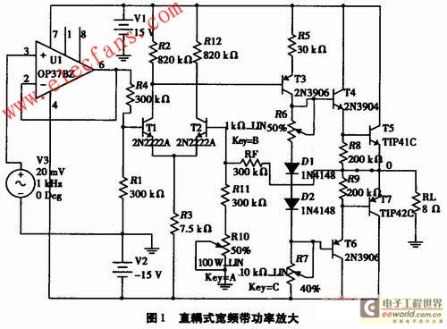
The main task of a direct-coupled broadband power amplifier is to provide the load with sufficiently large undistorted (or substantially undistorted) power. The entire circuit consists of three parts: input stage, pre-stage and output stage. The complete circuit is shown in Figure 1.

In the circuit of Figure 1, T1 and T2 form a long-tail differential amplifier with single-ended input and single-ended output, which mainly realizes the tasks of weak signal amplification and impedance matching. The integrated operational amplifier U1 at the front end of the differential amplifier is connected as a voltage follower to achieve impedance matching and avoid the influence of the internal resistance of the signal source on the static operating point; T3 and others constitute a common-emitter amplifier circuit to complete the driving task of the power amplifier stage; T4~T7 form a typical OCL power output stage.
The static operating point of the input stage is determined by R3, and the static collector current of transistors T1 and T2 is determined by the following formula:
The input stage signal amplitude is small, and the value of IC1 and IC2 is preferably about 1 mA. From formula (1), it can be seen that the value of R3 is 7.5 kΩ.
The static operating point of the pre-stage is related to the input stage. Assuming the collector point of T1 is UC1, the collector current of T3 is expressed by the following formula:
The output signal amplitude of the preamplifier can reach more than 10 V, requiring a larger dynamic range. If the output power is 5-10 W, 3 mA is more appropriate for IC3, considering both the dynamic range and the power consumption of T3. Under the circuit parameters shown in Figure 1, UC1 = 14.2 V, and the resistance of R5 should be about 30 Ω. Therefore, R5 is 30 Ω, and a precision linear adjustable potentiometer with a resistance of 100 Ω can be used.
The voltage gain of the entire channel is shared by the input stage and the pre-stage. RF, R10, R11, etc. form a voltage series negative feedback circuit. Under deep negative feedback conditions, the voltage gain of the entire channel is determined by the feedback coefficient:
R10 is a linear precision potentiometer, which is used to fine-tune the static operating point and compensate for the effect of the output resistance of the operational amplifier U1 on the static operating point. At the same time, the adjustment of R10 will also change the feedback coefficient of the circuit, thereby changing the output amplitude. The output power is adjusted by adjusting the input signal.
The frequency response of the circuit is determined by the inter-electrode capacitance of the transistor in the circuit and the frequency characteristics of the operational amplifier. The lower limit frequency of the circuit is 0, and the upper limit frequency of the circuit is mainly determined by the frequency characteristics of the power amplifier tube and the frequency characteristics of the operational amplifier. Selecting a power amplifier tube with a larger characteristic frequency and a high-speed broadband integrated operational amplifier can increase the upper limit frequency.
2 Multisim simulation of circuit performance
Multisim is an excellent EDA software with an intuitive and practical interface. In particular, the virtual electronic instruments in it have a one-to-one correspondence with the instruments in the laboratory. It is particularly suitable for simulation analysis of electronic circuits and is widely used in teaching, production, scientific research and other fields. Applying this software to this subject can achieve twice the result with half the effort.
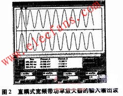
In the design process of this project, we used Multisim to simulate and analyze the circuit parameters, laying a foundation for hardware debugging and testing. The dynamic performance test of the circuit can be carried out on the premise of adjusting the static working point of the circuit. The signal source and oscilloscope in the software are called up, and the input and output waveforms are measured as shown in Figure 2 (the load resistance is 8 Ω). The upper part of the figure is the input signal waveform, and the lower part of the figure is the output signal waveform. It can be seen from the figure that when the output power is 9 W, the input signal is 20 mV, which can ensure that the input small signal can be effectively amplified and the circuit has sufficient sensitivity.

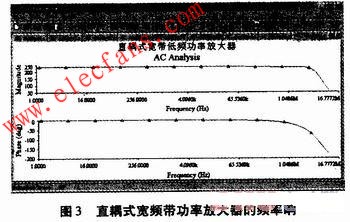
The measured frequency response of the circuit is shown in Figure 3 (the curve when the voltage gain is about 230). The upper part of the graph is the amplitude-frequency response, and the lower part of the graph is the phase-frequency response. It can be seen from the figure that the upper limit frequency is greater than 4 MHz, and the phase shift in the low frequency band is 0. Since the voltage gain is controlled by the negative feedback network, the passband width of the circuit is related to the gain of the circuit. The higher the gain, the narrower the frequency band. The simulation results show that when the output power is 2 W, the upper limit frequency of the circuit is greater than 2 MHz; when the output power is 9 W (the voltage gain is about 500), the upper limit frequency of the circuit is still greater than 100 kHz. According to different applications, it is necessary to reasonably select the output power and bandwidth. The maximum output power and bandwidth of the circuit are mainly adjusted by the feedback coefficient.

Applying Multisim for simulation analysis can provide direction for hardware debugging and improve work efficiency.
3 Circuit Hardware Debugging and Testing
3.1 Circuit Layout and Fabrication
The circuit discussed in this article includes both weak signal amplification circuits and large signal and high current circuits. The impact of the large current of the output stage on the weak signal circuit cannot be ignored. Therefore, circuit layout is very important, and making a printed circuit board is a better choice. If a universal version is used, the component layout and routing will have a particularly large impact on the circuit performance. The connection should be as short as possible, the ground wire should be as thick as possible (multiple strands in parallel), and attention should be paid to the decoupling of the power supply. Otherwise, the large current of the output stage will easily interfere with the input stage and cause the circuit to not work properly.
The parameters of the differential pair of tubes T1 and T2 should be as symmetrical as possible to ensure that the circuit has a good common-mode rejection ratio; asymmetric parameters of the output pair of tubes will cause waveform distortion, which should also be considered when selecting the output transistor; the withstand voltage of the transistor should also be paid attention to.
3.2 Debugging and adjustment of static working point
The circuit discussed in this article is a direct-coupled multi-stage amplifier. The static operating points are interrelated, making debugging difficult. Only by following the correct debugging steps and methods can success be achieved. Otherwise, it is easy to damage the transistors and cause failure.
In order to solve the problem of the connection between the front and back of the static operating point, RF can be disconnected from the output point 0, that is, the feedback loop can be disconnected to put the circuit in an open-loop state, thus avoiding the influence of the output stage on the static operating point of the previous stage (when the circuit is roughly adjusted, the voltage at the output point is generally deviated from the normal value). Of course, the influence of the previous stage on the next stage still exists, and the adjustment of the static operating point can be adjusted from the front to the back. After disconnecting the feedback loop, in order to simulate the static environment where the right end of RF is connected to point 0 (the static voltage value of point O is OV), the right end of RF can be temporarily connected to the ground. At the same time, in order to avoid the power amplifier tube being damaged during debugging and causing a chain reaction, the resistance value of R6 should be adjusted to O.
Short-circuit the input of operational amplifier U1 to ground, and adjust R10 to make the collector currents of T1 and T2 equal. At this time, the collector potential of T1 should be about 14.2 V (UC1=VCC-IC1R2), and the emitter potential of preamplifier tube T3 is about 14.9 V. Adjust R5 to make the collector current of T3 about 3 mA (see formula (2)), and then fine-tune R7 (R6, R7 are linear precision potentiometers) to make the collector potential UC3 of T3 about 0.7 V. At this time, the potential of output point O is 0 V. Change the right end of RF from ground to point O (closed loop), and fine-tune R7 to make the voltage at point O 0 V. The static operating point adjustment is complete.
3.3 Dynamic debugging and testing
Connect a small signal (frequency of 1 kHz, amplitude of 10 mV sine wave) to the input end, and observe the output signal with an oscilloscope under no-load and rated load conditions. The output signal should be a true sine wave. If crossover distortion occurs, R6 and R7 can be fine-tuned repeatedly to eliminate crossover distortion and ensure the correct static operating point.
Use a frequency characteristic tester or the "point frequency method" to measure the upper and lower limits of the circuit. By changing the models of the transistor (power amplifier tube) and operational amplifier U1, the upper limit frequency of the circuit will change accordingly, which is consistent with the results of theoretical calculations and software simulation.
It is worth noting that when testing the voltage amplification factor and frequency response of the circuit, when the load is connected, it is often accompanied by strong self-oscillation, making the test impossible. The solution is to connect a neutralizing and compensating capacitor (with a capacity of tens of picofarads to hundreds of picofarads) between the collector and base of several power amplifier tubes to eliminate the self-oscillation phenomenon.
4 Conclusion
(1) Experiments show that the output power of the circuit shown in Figure 1 can reach more than 10 W. By changing the power supply voltage, a higher output power can be obtained. The upper limit frequency varies greatly with the different models of power amplifier tubes and operational amplifiers U1. By selecting high-frequency high-power transistors and high-speed operational amplifiers, the upper limit frequency can reach more than 1 MHz.
(2) The circuit shown in Figure 1 can be applied to audio amplifiers and can also be applied to the amplification channel of a signal generator.
(3) The simulation analysis and hardware debugging methods introduced in this paper are suitable for engineering application fields such as TTL, OCL and other power amplifier circuits and IC design.
Previous article:Golden Rules for Effectively Simplifying Isolation Amplifier Design in Analog Signal Isolation Applications
Next article:Principle and Application of Zero-Drift Amplifier
- High signal-to-noise ratio MEMS microphone drives artificial intelligence interaction
- Advantages of using a differential-to-single-ended RF amplifier in a transmit signal chain design
- ON Semiconductor CEO Appears at Munich Electronica Show and Launches Treo Platform
- ON Semiconductor Launches Industry-Leading Analog and Mixed-Signal Platform
- Analog Devices ADAQ7767-1 μModule DAQ Solution for Rapid Development of Precision Data Acquisition Systems Now Available at Mouser
- Domestic high-precision, high-speed ADC chips are on the rise
- Microcontrollers that combine Hi-Fi, intelligence and USB multi-channel features – ushering in a new era of digital audio
- Using capacitive PGA, Naxin Micro launches high-precision multi-channel 24/16-bit Δ-Σ ADC
- Fully Differential Amplifier Provides High Voltage, Low Noise Signals for Precision Data Acquisition Signal Chain
- Innolux's intelligent steer-by-wire solution makes cars smarter and safer
- 8051 MCU - Parity Check
- How to efficiently balance the sensitivity of tactile sensing interfaces
- What should I do if the servo motor shakes? What causes the servo motor to shake quickly?
- 【Brushless Motor】Analysis of three-phase BLDC motor and sharing of two popular development boards
- Midea Industrial Technology's subsidiaries Clou Electronics and Hekang New Energy jointly appeared at the Munich Battery Energy Storage Exhibition and Solar Energy Exhibition
- Guoxin Sichen | Application of ferroelectric memory PB85RS2MC in power battery management, with a capacity of 2M
- Analysis of common faults of frequency converter
- In a head-on competition with Qualcomm, what kind of cockpit products has Intel come up with?
- Dalian Rongke's all-vanadium liquid flow battery energy storage equipment industrialization project has entered the sprint stage before production
- Allegro MicroSystems Introduces Advanced Magnetic and Inductive Position Sensing Solutions at Electronica 2024
- Car key in the left hand, liveness detection radar in the right hand, UWB is imperative for cars!
- After a decade of rapid development, domestic CIS has entered the market
- Aegis Dagger Battery + Thor EM-i Super Hybrid, Geely New Energy has thrown out two "king bombs"
- A brief discussion on functional safety - fault, error, and failure
- In the smart car 2.0 cycle, these core industry chains are facing major opportunities!
- The United States and Japan are developing new batteries. CATL faces challenges? How should China's new energy battery industry respond?
- Murata launches high-precision 6-axis inertial sensor for automobiles
- Ford patents pre-charge alarm to help save costs and respond to emergencies
- New real-time microcontroller system from Texas Instruments enables smarter processing in automotive and industrial applications
- Lots of books! Have you read any books on this Book Day? Have you bought any books?
- What does Dual Panel Flash mean in the introduction of ATSAMD51P20A?
- Capacitor three-point oscillation composed of operational amplifier
- 09 ADC acquisition and power management system (series post)
- 【Short-term weather forecast system】Scheme planning
- 【GD32450I-EVAL】Preliminary Study on TLI-RGB Screen Driver
- An easy-to-understand tutorial on the msp430 microcontroller
- [TI recommended course] #PFC power supply design and inductor design calculation#
- [Distributed temperature and humidity acquisition system] + STM32H745I-LWIP program
- Summary: TI LAUNCHXL-CC2650 evaluation report

 ICCV2023 Paper Summary: Humans, 3D Modeling, and Driving
 EMC test standard: ISO 7637-2:2011(E)


 京公网安备 11010802033920号