Overview
An ideal digital-to-analog converter (DAC) has an ideal linear relationship between its output voltage or current and input, and is not affected by other external factors (such as temperature). Of course, in practical applications, DACs are inevitably affected by various external factors and errors occur. Temperature is an obvious factor, and the DAC output will drift with temperature changes. This is especially important when using a high-precision DAC to accurately establish the bias voltage. We can calibrate all static drifts, but it is difficult to compensate for the part that changes with temperature. The errors caused by temperature are mainly: offset error and gain error.
This application note describes how to determine the relationship between the DAC's offset error and gain error and temperature, helping designers to anticipate these error factors during the design process. Having this knowledge also helps ensure that the system meets the specification requirements in terms of temperature characteristics.
Offset and Gain Errors
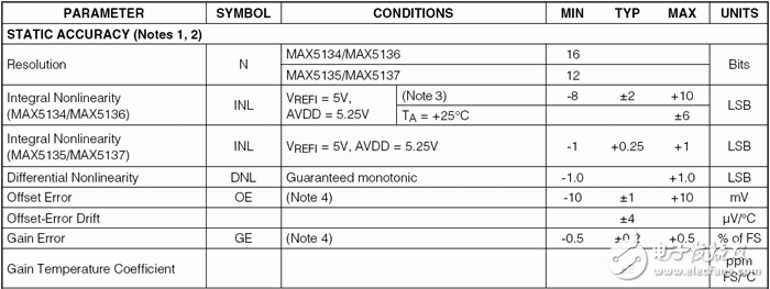
As mentioned above, many error factors affect DAC performance, such as offset error and gain error, and the impact of these factors is shown in the "static accuracy" parameter section of the DAC device data sheet. Figure 1 shows the specifications of the MAX5134 16-bit, 4-channel DAC.

Note 4: Gain and offset tests, test points are at 100mV and AVDD
Figure 1. Offset and gain errors of the MAX5134.
What do these parameters mean for DAC performance?
The offset error is usually defined at the output of the device at the zero point. For unipolar output, this value is the output corresponding to zero code, usually called zero code error; for bipolar output, it is defined at the DAC output corresponding to the intermediate code value.
Gain error is the slope of the transfer function, which for the MAX5134 is between 99.5% and 100.5% of the theoretical value.
Figure 2 shows the offset error and gain error. Note that the offset and gain errors can be positive or negative.

Figure 2 Offset and gain errors.
Normally we do not measure offset and gain errors directly. If a unipolar device exhibits a negative offset error, the test result at zero code is obviously incorrect. Because unipolar DACs are usually powered by a single positive power supply, the DAC will not be able to produce negative values. You can test two points and then calculate the offset and gain errors. One test point is close to zero code, and the other test point is close to the maximum code value or even at the maximum code value. For the MAX5134, you can choose two test points, 100mV and power supply AVDD. The test conditions are shown in Note 4 of Figure 1 (Note 4: Gain and offset test, test points are located at 100mV and AVDD, see the MAX5134 data sheet, which can be downloaded from the Maxim website).
Next, consider the effect of temperature. Both offset error and gain error will drift with temperature changes. For applications that use DACs to accurately set bias voltages, the impact of temperature drift is even greater. If the offset and gain errors are fixed, they can be calibrated through a variety of techniques, some of which can be referenced). In general, temperature drift calibration is a very complex task. First, the temperature needs to be measured, and then the corresponding compensation is taken according to the temperature value.
Calculation Examples and Typical Results
Here we take MAX5134 as an example. By evaluating a large number of devices, we can get the maximum static error. We first define several concepts or equations to calculate the error range.
VOUT = N × G × (GE + GET) + OE + OET

| Here: | VOUT = Output voltage |
| N = DAC input code value | |
| G = DAC gain | |
| GE = DAC gain error | |
| GET = Additional gain error due to temperature variation | |
| OE = DAC offset error | |
| OET = Additional offset error due to temperature variation | |
| VREF = reference voltage | |
| NMAX = DAC maximum code value |
The offset error drift of the parameter is ±4µV/°C, using the box method. To determine the temperature offset, the temperature drift coefficient can be multiplied by the temperature range. Note that the temperature range here refers to the specified operating temperature range of the device, not the actual application temperature range. In this case, it is -40°C to +105°C, and the offset drift caused by temperature is ±0.58mV. Similarly, the gain temperature drift coefficient is 2ppm/°C, which is equivalent to ±0.029%FS (full scale).
For the first example, we use a 2.5V reference voltage VREF and the DAC is a 16-bit device, that is, the maximum code value NMAX is 65535.
Another issue is ease of use. It is best to specify offset and gain errors as "minimum/maximum" values, while temperature effects can only be defined as typical values. We can use typical values or estimate the variation over the entire range based on experience. Typical values are used here.
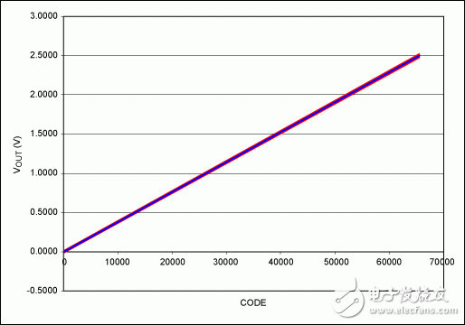
The curve shown in Figure 3 is the relationship between the initial error output voltage and the input code. This is a characteristic curve of an actual DAC device. This set of curves is closer than Figure 2 and is not easy to analyze, so it is best to plot the deviation between them and the ideal curve, as shown in Figure 4. Figure 4 also shows the overall error including the temperature effect.

Figure 3. DAC output vs. input code plot shows the effects of gain and offset errors for a 2.5V reference.

Figure 4. DAC output error vs. input code for a 2.5V reference.
As can be seen from the figure, the effect of temperature is much lower than the initial error, so even if the data sheet only gives the typical value of the temperature characteristics, it will not have a significant impact on the overall error. The overall error at zero code is ±0.423%FS (±10.6mV), and the overall error at the maximum input code is ±0.952%FS (±23.8mV).
Some improvement measures can be taken, such as increasing the reference voltage. Since the gain error is specified as a percentage of the full scale (%FS), its absolute value will increase, but the absolute value of the offset error will not increase. Therefore, the full-scale output voltage can be increased by increasing the reference voltage, and then the DAC output can be reduced to the required voltage externally. In this way, the gain error is restored to its original value, while the offset error can be reduced. Figure 5 shows the effect of this method.

Figure 5. Example of DAC output error vs. input code for a 2.5V reference.
At zero code, the overall error is ±0.212%FS (±5.3mV); at maximum code, the overall error is ±0.740%FS (±18.5mV).
Of course, this result ignores the error introduced by the output voltage divider. However, this method is completely feasible because the output voltage divider can use a precision voltage divider, such as the MAX5490, whose ratio accuracy temperature characteristics can reach ±0.05%. Of course, the disadvantage of dividing the DAC output is that the drive capability is reduced, and the output drive needs to be improved by an op amp, which will introduce additional errors. An in-depth discussion of this method is beyond the scope of this article.
in conclusion
This article discusses the effects of offset error and gain error on DAC accuracy. It also gives examples of how to calculate the worst-case error and provides some suggestions for improving the overall error.
Previous article:MAX2982 Industrial Broadband Powerline Modem
Next article:Wireless Communication RF Direct Conversion Transmitter
Recommended ReadingLatest update time:2024-11-16 15:57


- Popular Resources
- Popular amplifiers
-
 【Follow me Season 2 Episode 2】Arduion UR4 homework submission code
 -
 MCU C language programming and Proteus simulation technology (Xu Aijun)
 -
 100 Examples of Microcontroller C Language Applications (with CD-ROM, 3rd Edition) (Wang Huiliang, Wang Dongfeng, Dong Guanqiang)
 -
 Principles and Applications of Single Chip Microcomputers 3rd Edition (Zhang Yigang)
- High signal-to-noise ratio MEMS microphone drives artificial intelligence interaction
- Advantages of using a differential-to-single-ended RF amplifier in a transmit signal chain design
- ON Semiconductor CEO Appears at Munich Electronica Show and Launches Treo Platform
- ON Semiconductor Launches Industry-Leading Analog and Mixed-Signal Platform
- Analog Devices ADAQ7767-1 μModule DAQ Solution for Rapid Development of Precision Data Acquisition Systems Now Available at Mouser
- Domestic high-precision, high-speed ADC chips are on the rise
- Microcontrollers that combine Hi-Fi, intelligence and USB multi-channel features – ushering in a new era of digital audio
- Using capacitive PGA, Naxin Micro launches high-precision multi-channel 24/16-bit Δ-Σ ADC
- Fully Differential Amplifier Provides High Voltage, Low Noise Signals for Precision Data Acquisition Signal Chain
- Innolux's intelligent steer-by-wire solution makes cars smarter and safer
- 8051 MCU - Parity Check
- How to efficiently balance the sensitivity of tactile sensing interfaces
- What should I do if the servo motor shakes? What causes the servo motor to shake quickly?
- 【Brushless Motor】Analysis of three-phase BLDC motor and sharing of two popular development boards
- Midea Industrial Technology's subsidiaries Clou Electronics and Hekang New Energy jointly appeared at the Munich Battery Energy Storage Exhibition and Solar Energy Exhibition
- Guoxin Sichen | Application of ferroelectric memory PB85RS2MC in power battery management, with a capacity of 2M
- Analysis of common faults of frequency converter
- In a head-on competition with Qualcomm, what kind of cockpit products has Intel come up with?
- Dalian Rongke's all-vanadium liquid flow battery energy storage equipment industrialization project has entered the sprint stage before production
- Allegro MicroSystems Introduces Advanced Magnetic and Inductive Position Sensing Solutions at Electronica 2024
- Car key in the left hand, liveness detection radar in the right hand, UWB is imperative for cars!
- After a decade of rapid development, domestic CIS has entered the market
- Aegis Dagger Battery + Thor EM-i Super Hybrid, Geely New Energy has thrown out two "king bombs"
- A brief discussion on functional safety - fault, error, and failure
- In the smart car 2.0 cycle, these core industry chains are facing major opportunities!
- The United States and Japan are developing new batteries. CATL faces challenges? How should China's new energy battery industry respond?
- Murata launches high-precision 6-axis inertial sensor for automobiles
- Ford patents pre-charge alarm to help save costs and respond to emergencies
- New real-time microcontroller system from Texas Instruments enables smarter processing in automotive and industrial applications

 【Follow me Season 2 Episode 2】Arduion UR4 homework submission code
 MCU C language programming and Proteus simulation technology (Xu Aijun)


 京公网安备 11010802033920号