According to the working principle of the instrumentation amplifier, a low-frequency weak signal amplification circuit is designed using
the TLC2652 of
Texas Instruments
. Through Multisim software simulation analysis, the circuit has extremely high input resistance, extremely low output resistance, strong common-mode suppression ability, can amplify microvolt signals with a frequency of 0 to 300 Hz, and the circuit works stably with low distortion. This paper mainly designs a weak signal amplifier with DC and low-frequency signals as the research objects, and performs simulation analysis.
1 Selection of integrated operational amplifiers
With the development of integrated technology and electronic technology, the performance of integrated operational amplifiers is getting better and better. TLC2652 is a high-precision chopper-stabilized operational amplifier produced by Texas Instruments using advanced LinCMOS technology. The chopper-stabilized technology gives TLC2652 excellent DC characteristics, which reduces the impact of offset voltage and its drift, common-mode voltage, low-frequency noise, power supply voltage changes, etc. on the operational amplifier to a minimum, so TLC2652 is very suitable for micro-signal amplification.
1.1 Internal structure of TLC2652
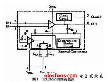
As shown in Figure 1, TLC2652 is mainly composed of 5 functional modules:

(1) Main amplifier: Unlike general operational amplifiers, it has three input terminals. In addition to the in-phase and inverting input terminals that are led out of the chip, it also has a in-phase input terminal for zero calibration inside the chip.
(2) Null amplifier: It also has three input terminals, but unlike the main amplifier, the input terminal inside the chip is the inverting input terminal.
(3) Clock and switch circuit: The internal clock generates a clock signal to control the closing and opening of each switch in a certain timing sequence. In the 14- and 20-pin chips, the clock signal can also be introduced from the outside.
(4) Compensation network (Compensation-Basing Circuit): It makes the circuit have a flat response within a wider frequency band. In TLC2652, the high-frequency response of the circuit is mainly determined by the main amplifier.
(5) Clamp Circuit: It is actually a switch that operates when the output voltage is close to 1 V different from the power supply voltage. When the CLAMP is short-circuited with the inverting input terminal of the op amp, the deep negative feedback introduced can greatly reduce the gain of the circuit when it is overloaded to prevent saturation. It can accelerate the recovery of the circuit after overload.
1.2 Main performance indicators of TLC2652
(1) Extremely low input offset voltage: maximum value 1μv
(2) Extremely low input offset voltage drift: typical value 0.003μV/℃
(3) Low input offset current: maximum value 500pA (TA=-55℃~125℃)
(4) Open-loop voltage gain: minimum value 135dB
(5) Common mode rejection ratio: minimum value 120dB
2 Weak signal amplifier circuit
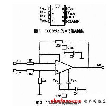
The typical circuit of TLC2652 is shown in Figure 3, which constitutes a differential amplifier circuit.

If R1=R2, R3=R4, then
u0=(ui1-ui2)(R2/R1)
This circuit provides the function of instrumentation amplifier, i.e. amplifying differential signal while suppressing common mode signal, but the impedance of in-phase input and inverting input is quite low and unequal. It is easy to get from Figure 3 that the impedance of in-phase input is (R2+R4), and the impedance of inverting input is R1. In addition, this circuit requires that the ratio of resistors R1/R2 and R3/R4 is matched very precisely, otherwise, the gain of each input will be different, which will directly affect the CMR of the circuit. Now, according to the working principle of instrumentation amplifier, a high-precision and high-stability amplifier is designed.
2.1 Working Principle of Instrumentation Amplifier
The circuit of a standard three-op-amp instrumentation amplifier is shown in Figure 4. This circuit can provide high impedance matching at both input ends, so that the input source impedance has the least effect on the CMR of the circuit. The A1 and A2 operational amplifiers are used to buffer the input voltage, and A3 constitutes a differential amplifier circuit.

As shown in the circuit in Figure 4, if R5=R6, R1=R2 and R3=R4, then
u0=(ui2-ui1)(1+2R5/RG)(R3/R1)
If A1 and A2 use the same operational amplifier, their common-mode output voltage and drift voltage are equal, and after being added to the differential amplifier A3, they will be offset each other. Therefore, the whole circuit has a strong common-mode suppression capability, a small input offset voltage and a high differential-mode voltage gain.
2.2 Circuit Schematic Diagram
According to the principle of instrumentation amplifier, a weak signal amplification circuit composed of TLC2652 is designed as shown in Figure 5.

As shown in Figure 5, two TLC2652s are used to realize input buffering. TLC2652 has extremely small input offset voltage, and the common-mode output voltage is equal. Low-noise, low-input bias current OP1177 is used as a differential amplifier circuit. Capacitors C1, C2, C3, and C4 are connected to the CxA and CxB pins of TLC2652 as memory capacitors to store offset voltages to achieve zero calibration. Capacitors C5, C6, C7, C8, and C9 are used as power supply filter capacitors to filter out high-frequency interference. According to the working principle of the instrumentation amplifier, the gain of the circuit is G=(1+2X300/2)(100/10)=3010.
3 Simulation Analysis
Based on the weak signal amplifier circuit, the circuit was built in Multisim10.0 software for simulation analysis. Assuming the frequency of the input signal is 60 Hz, the amplitudes of ui1 and ui2 are both 10μVp, and using Transient Analysis, the output waveform of the circuit can be obtained as shown in Figure 6. By dragging the ruler, we can calculate that the circuit gain G is about 3000, or 69.5dB.
Run ACAnalysis under Analysis to get the frequency characteristic curve shown in Figure 7. From this figure, we can see that the amplitude-frequency characteristic and phase-frequency characteristic of the amplifier circuit are relatively stable at medium and low frequencies. By dragging the ruler, we can get that the bandwidth of the circuit is about 300Hz.

The simulation measurement using Multisim software also shows that the input resistance of the circuit is very large, about tens of MΩ; the output resistance is very small, less than 1Ω; the common mode rejection ratio can reach more than 60dB; the circuit distortion rate is less than 0.05%; the frequency stability is less than 0.02% within a bandwidth of 300Hz.
4 Conclusion
This paper designs a weak signal amplification circuit for low-frequency signals using TLC2652, and uses Multisim software for simulation analysis. The analysis results show that all indicators meet the design requirements and have certain application value in practice. However, making a physical circuit will inevitably introduce some noise, such as the wiring of the PCB board and the selection of materials need to be paid attention to.
Previous article:Best experience in analog design
Next article:A digital power amplifier PCB implementation solution
- High signal-to-noise ratio MEMS microphone drives artificial intelligence interaction
- Advantages of using a differential-to-single-ended RF amplifier in a transmit signal chain design
- ON Semiconductor CEO Appears at Munich Electronica Show and Launches Treo Platform
- ON Semiconductor Launches Industry-Leading Analog and Mixed-Signal Platform
- Analog Devices ADAQ7767-1 μModule DAQ Solution for Rapid Development of Precision Data Acquisition Systems Now Available at Mouser
- Domestic high-precision, high-speed ADC chips are on the rise
- Microcontrollers that combine Hi-Fi, intelligence and USB multi-channel features – ushering in a new era of digital audio
- Using capacitive PGA, Naxin Micro launches high-precision multi-channel 24/16-bit Δ-Σ ADC
- Fully Differential Amplifier Provides High Voltage, Low Noise Signals for Precision Data Acquisition Signal Chain
- Innolux's intelligent steer-by-wire solution makes cars smarter and safer
- 8051 MCU - Parity Check
- How to efficiently balance the sensitivity of tactile sensing interfaces
- What should I do if the servo motor shakes? What causes the servo motor to shake quickly?
- 【Brushless Motor】Analysis of three-phase BLDC motor and sharing of two popular development boards
- Midea Industrial Technology's subsidiaries Clou Electronics and Hekang New Energy jointly appeared at the Munich Battery Energy Storage Exhibition and Solar Energy Exhibition
- Guoxin Sichen | Application of ferroelectric memory PB85RS2MC in power battery management, with a capacity of 2M
- Analysis of common faults of frequency converter
- In a head-on competition with Qualcomm, what kind of cockpit products has Intel come up with?
- Dalian Rongke's all-vanadium liquid flow battery energy storage equipment industrialization project has entered the sprint stage before production
- Allegro MicroSystems Introduces Advanced Magnetic and Inductive Position Sensing Solutions at Electronica 2024
- Car key in the left hand, liveness detection radar in the right hand, UWB is imperative for cars!
- After a decade of rapid development, domestic CIS has entered the market
- Aegis Dagger Battery + Thor EM-i Super Hybrid, Geely New Energy has thrown out two "king bombs"
- A brief discussion on functional safety - fault, error, and failure
- In the smart car 2.0 cycle, these core industry chains are facing major opportunities!
- The United States and Japan are developing new batteries. CATL faces challenges? How should China's new energy battery industry respond?
- Murata launches high-precision 6-axis inertial sensor for automobiles
- Ford patents pre-charge alarm to help save costs and respond to emergencies
- New real-time microcontroller system from Texas Instruments enables smarter processing in automotive and industrial applications
- Ten important facts and trends in motor control
- Surge protection for MOSFET DC switches
- #The best content of the "Interview with famous teachers" in the electronic competition#The first issue - Professor Hu Renjie of Southeast University
- BlueNRG-LP uses RNG function in static protocol stack and cannot broadcast
- Power Supply Ripple Measurement Setup (Oscilloscope)
- c8051F060 program download problem
- 1
- Thermistor, hysteresis resistor, gas resistor, varistor, photoresistor application circuit collection
- Can a bandpass filter be powered from a single supply?
- Discussion on Graphical Programming Method of Single Chip Microcomputer

 New concept analog circuits, 5 parts in total - Yang Jianguo
 Electrostatic Discharge (ESD) Design Guidelines


 京公网安备 11010802033920号