ADSP21160 adopts super Harvard structure and has 4 independent buses in the chip, which are used for dual data access, instruction access and input/output interface respectively. The chip integrates the main functional blocks of digital information processing system such as processor core (including operation unit, control unit, address generator and bus, interrupt, register, etc.), large-capacity dual-port static memory, program/data external bus and multi-processor interface, input/output controller, etc.
Hardware system design ideas
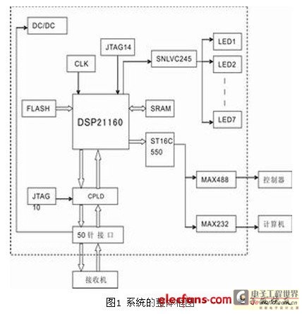
The following briefly introduces the system design ideas from the aspects of data input and output, system power-on operation, system power supply configuration and circuit control.
1. First consider data transmission. The external device (receiver) converts the data into serial data output after being processed by ADSP21160 through the 50-pin interface and transmits it to the peripheral device (controller) and computer. In order to ensure the confidentiality of the circuit system and facilitate the implementation of some logic control circuits in the system, a CPLD control circuit is added between ADSP21160 and the 50-pin interface.
2. In order for the system to run automatically after power-on, it is necessary to configure an external FLASH for the DSP and pre-burn the calculation program into the FLASH. By configuring the boot mode of ADSP21160, after the system is powered on, ADSP21160 can automatically read the program from the FLASH and run it.
3. Since ADSP21160 has only 4Mbit of internal storage space, which is equally divided into data storage space and program storage space. In order to facilitate future upgrades of the system and programs, 512K×32-bit external storage space is configured using SRAM.
4. Since the serial port of ADSP21160 is not a universal UART serial port, and both the system and the computer require serial data output, a parallel-to-serial conversion chip is needed in the system to output the calculation results.
5. Since only +5V DC power is provided externally, and ADSP21160 requires +3.3V interface power and 2.5V core power, the internal components of the system should also choose +3.3V devices accordingly. Therefore, the system needs a DC/DC conversion chip to convert the +5V power supply into +2.5V and +3.3V power outputs.
Design of each functional module of the system
1. Power module design
In the design of the system, since the external interface power supply of ADSP21160 is +3.3V, in order to simplify the circuit and improve the performance of the circuit board, +3.3V devices are also selected as much as possible in the selection of other devices. For a few devices that are difficult to find +3.3V power supply, +5V devices are selected without affecting the interface and function. In addition, ADSP21160 also requires +2.5V core power supply and +2.5V analog power supply (for the internal phase-locked loop of ADSP21160). The external power supply to the system is +5V. Considering the above requirements, the system needs a DC/DC conversion module to output +3.3V and +2.5V voltages, and divide the +2.5V power supply into digital and analog.
ADSP21160 requires the core power supply to be earlier than the external port power supply, otherwise it may cause abnormal startup of DSP or failure to load the program. Therefore, this problem is taken into consideration in the power supply design, and it is decided to use the +2.5V output end of the DC/DC to connect to the +3.3V output enable end through a delay circuit, which solves this problem well.
Considering the specific requirements of the system for voltage and current, this hardware system selects TI's TPS767D301 as the DC/DC conversion chip. Its input is +5V voltage, and it outputs a +3.3V voltage and a +1.8V or +2.5V adjustable voltage, with a maximum current output of 1A.
2.DSP main module design
Clock drive: ADSP21160 needs external clock drive, so external clock is essential. Its unique internal phase-locked loop setting can multiply the internal operation frequency to 2, 3 or 4 times the external clock frequency, and the highest core clock frequency is 80MHz. In this way, the core processor can run at a high speed when the external frequency (data transmission frequency) is low.
In this system, in order to improve the system's high-frequency interference capability and reduce the difficulty of system design, without having much impact on the system's operating speed (since the system's main time consumption is concentrated on matrix processing operations, data transmission relatively only accounts for a few tenths of its total operating time), an external 20MHz drive clock was selected, and the internal phase-locked loop was set to 4 times the external clock to achieve internal high-speed computing.
Program loading: ADSP21160 requires an external 14-pin JTAG interface. By using the ICE emulator provided by ADI, the compiled user program is downloaded from the computer and loaded into the internal memory of ADSP21160 or the external FLASH.
External device selection: ADSP21160 is equipped with four external pins /MS3~/MS0 for external device selection. At the same time, only one of them is allowed to be valid (low level). These pins are respectively connected to the enable end of FLASH, SRAM, and parallel-to-serial conversion chip (ST16C550) to select these components and for data communication with external receivers. CPLD is in working state for a long time (the enable end is directly grounded) because it is related to the logical functions of several devices.
3.FLASH loading and external memory module design
FLASH loading module: In order for the system to run automatically after power-on, an external FLASH is configured for ADSP21160. According to the user manual of ADSP21160, the data line of 8-bit FLASH is connected to the 32_39 bits of DSP data line, and the address line must be directly connected to the corresponding address bit of ADSP21160 starting from ADDR0. ADSP21160 adopts EPROM startup mode, and /BMS and /MS0 are connected to the enable end of FLASH.

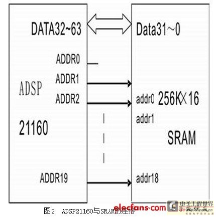
External memory module: ADSP21160 is a high-performance 32-bit floating-point processor, which can use a 64-bit data bus at most. Considering the accuracy requirements of the system and the processing mode of internal data, this system only uses a 32-bit data bus for external use. In this way, in the selection of external memory, considering factors such as price, two 256K×16-bit SRAMs are selected in parallel to form a 32-bit external memory, as shown in Figure 2.

The connection of the address line is slightly different from the general connection method. As ADSP21160 stipulates, for addressing the external space, the odd address is transmitted through the lower 32-bit data line; the even address is transmitted through the upper 32-bit data line. Considering that 32_39 bits of the DSP data line are used in the connection of FLASH, in order to simplify the wiring of the PCB board in the future and make full use of the storage space of SRAM, in the design, the ADDR0 pin of ADSP21160 is left floating, and its ADDR1 pin is connected to the addr0 pin of SRAM, ADDR2 is connected to addr1, and the following connections are made in sequence.
External communication interface module design
The target board is connected to the receiver through a 50-pin interface, and reads data from the storage space opened up inside the receiver through four control signal lines: RD_REQ, RD_PMT, RD_EN, and RD_CLK.
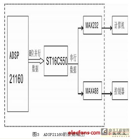
In the design of this system, the intermediate operation data are all 32-bit floating point numbers, and the output results are truncated to 8 effective digits, which are converted into serial data through a parallel-to-serial converter (ST16C550), and then divided into two paths. One path is converted into differential data by MAX488 and transmitted to an external controller, and the other path is converted by MAX232 and connected to a computer, realizing the functions required by the system, as shown in Figure 3.

Conclusion
ADSP21160 is powerful, but slightly complicated in power configuration. This system uses 2.5V power output as 3.3V output enable, successfully solving this problem. In addition, on the basis of meeting system requirements, in order to reduce the difficulty of design, special designs are made for clock and data lines. The clock uses an off-chip medium and low frequency (20MHz) and is multiplied to the maximum frequency (80MHz) on the chip, which reduces the requirements for medium and high frequency wiring on the PCB board; the data line reduces the off-chip line width from 64 bits to 32 bits by leaving the 0-bit address dangling, which greatly reduces the line density around the ADSP21160, thereby greatly reducing the difficulty of PCB board wiring.
Previous article:Realization of the method of detecting sound with microwaves
Next article:Design of optical imaging system of fully automatic focal meter based on CCD
- High signal-to-noise ratio MEMS microphone drives artificial intelligence interaction
- Advantages of using a differential-to-single-ended RF amplifier in a transmit signal chain design
- ON Semiconductor CEO Appears at Munich Electronica Show and Launches Treo Platform
- ON Semiconductor Launches Industry-Leading Analog and Mixed-Signal Platform
- Analog Devices ADAQ7767-1 μModule DAQ Solution for Rapid Development of Precision Data Acquisition Systems Now Available at Mouser
- Domestic high-precision, high-speed ADC chips are on the rise
- Microcontrollers that combine Hi-Fi, intelligence and USB multi-channel features – ushering in a new era of digital audio
- Using capacitive PGA, Naxin Micro launches high-precision multi-channel 24/16-bit Δ-Σ ADC
- Fully Differential Amplifier Provides High Voltage, Low Noise Signals for Precision Data Acquisition Signal Chain
- Innolux's intelligent steer-by-wire solution makes cars smarter and safer
- 8051 MCU - Parity Check
- How to efficiently balance the sensitivity of tactile sensing interfaces
- What should I do if the servo motor shakes? What causes the servo motor to shake quickly?
- 【Brushless Motor】Analysis of three-phase BLDC motor and sharing of two popular development boards
- Midea Industrial Technology's subsidiaries Clou Electronics and Hekang New Energy jointly appeared at the Munich Battery Energy Storage Exhibition and Solar Energy Exhibition
- Guoxin Sichen | Application of ferroelectric memory PB85RS2MC in power battery management, with a capacity of 2M
- Analysis of common faults of frequency converter
- In a head-on competition with Qualcomm, what kind of cockpit products has Intel come up with?
- Dalian Rongke's all-vanadium liquid flow battery energy storage equipment industrialization project has entered the sprint stage before production
- Allegro MicroSystems Introduces Advanced Magnetic and Inductive Position Sensing Solutions at Electronica 2024
- Car key in the left hand, liveness detection radar in the right hand, UWB is imperative for cars!
- After a decade of rapid development, domestic CIS has entered the market
- Aegis Dagger Battery + Thor EM-i Super Hybrid, Geely New Energy has thrown out two "king bombs"
- A brief discussion on functional safety - fault, error, and failure
- In the smart car 2.0 cycle, these core industry chains are facing major opportunities!
- The United States and Japan are developing new batteries. CATL faces challenges? How should China's new energy battery industry respond?
- Murata launches high-precision 6-axis inertial sensor for automobiles
- Ford patents pre-charge alarm to help save costs and respond to emergencies
- New real-time microcontroller system from Texas Instruments enables smarter processing in automotive and industrial applications
- EEWORLD University Hall----Live Replay: Wireless Technology Changes Smart Life
- I bought a few cheap wireless charging receiver modules.
- EEWORLD University ---- Yunlong 51 MCU video tutorial
- Talk about the processing of Buck circuit in complex environment
- [A must-read for electrical engineers] In 3 minutes, we will reveal the past and present of commonly used electrical measurement units!
- Where will nanotechnology, the Internet of Things and Industry 4.0 meet?
- Problems encountered in device EMC and RF testing
- Free Review | Espressif Audio Development Board: ESP32-Korvo
- Several LM386 audio amplifier circuits shared
- NXP MKL25Z128 + LCD

 Accurate Level-crossing ADC Design for Biomedical Acquisition


 京公网安备 11010802033920号