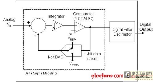
The delta-sigma ADC may look complex on the surface, but it is actually a series of simple components that make up a precise data converter. The delta-sigma ADC consists of two main building blocks: a delta-sigma modulator that performs the analog-to-digital conversion and a digital low-pass filter/decimation circuit. The basic building blocks of the delta-sigma modulator (integrated op amp, summing node, comparator/1-bit ADC, and 1-bit DAC) are shown in Figure 1. The modulator's charge balancing circuit forces the comparator's digital output bit stream to represent the average analog input signal. The comparator output is processed by a low-pass digital filter while being fed back to the modulator's 1-bit DAC. This filter essentially counts the number of 0s and 1s and removes much of the noise, allowing for data converters up to 24 bits.

Figure 1: A delta-sigma ADC consists of a delta-sigma modulator that performs the analog-to-digital conversion followed by a digital filter and decimator.
analog: simulation
integrator: integrator
comparator: Comparator
1-bit ADC:1 位 ADC
digital filter: digital filter
decimator: extractor
digital output: digital output
1-bit DAC: 1-bit DAC
1-bit data stream: 1-bit data stream
A major obstacle to achieving more bits of resolution is noise. Noise can be a major problem for designers trying to discern microvolt (μV) changes from thermocouples, sensors, or other low-level signal sources. The noise floor is composed of the sum of all the unwanted external and modulator-surrounding noise sources. And the thicker the noise floor, the harder it is to detect real changes in the analog input signal you are trying to test.
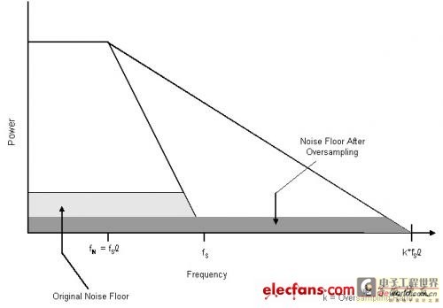
Oversampling, noise shaping, digital filtering, and decimation are four important methods that delta-sigma converters use to reduce noise and produce high-resolution output data. Assuming that a data converter's input signal is sampled at a frequency fS, according to the Nyquist theorem for data, fS must be at least twice the input frequency (fIN=fS/2). Oversampling is sampling the input signal at a frequency that is twice the input signal frequency. A larger oversampling ratio (k) will produce a more complete digital bit stream representation. The more "1" or "0" that make up the bit stream, the better the digital approximation of the input signal. Figure 2 shows how oversampling at a sampling rate of kx fS/2 allows the modulator to spread the same amount of noise over a wider frequency range. This greatly reduces the noise floor in the frequency band of interest. For every 2x increase in the oversampling ratio, the ideal signal-to-noise ratio (SNR) improves by 3dB. A larger SNR means that the delta-sigma converter can better resolve smaller changes in the analog input.

Figure 2: Oversampling reduces the noise floor in the frequency band of interest
Power: Power
Noise floor after oversampling: Noise floor after oversampling
orignal noise floor: initial noise layer
frequency: frequency
Oversampling ratio: oversampling ratio
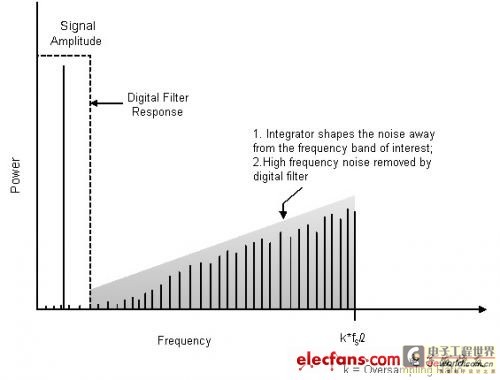
The delta-sigma converter can accurately measure the analog input by using an integrator in the modulator control loop to perform noise shaping. The noise shaping process of the integrator is to force more noise to higher frequencies, as shown in Figure 3. The digital low-pass filter then removes the high frequency portion of the noise, which greatly improves the SNR. The digital filter can also be used to greatly reduce noise at 50Hz, 60Hz or other unwanted frequencies.

Figure 3: The integrator forces the noise to a higher frequency
Signal Amplitude : Signal amplitude
Digital Filter Rsponse: Digital filter response
power: power
1. The integrator forces the noise out of the frequency band of interest;
2. Digital filter filters out high-frequency noise
frequency: frequency
Oversampling ratio: oversampling ratio
There will always be some noise in the digital bit stream from the input signal. But through averaging and filtering, delta-sigma ADCs significantly reduce the noise floor. The oversampling ratio and the "order" of the internal delta-sigma modulator determine the noise level. The term order refers to the number of integrators. For example, a 3rd order modulator has 3 integrator stages.
Although adding integrator stages and increasing oversampling ratios can further reduce noise, stability is a major concern for 3rd-order or higher delta-sigma converters. Once delta-sigma modulators become unstable, they often do not become stable again unless power is cycled. All Linear Technology delta-sigma converters use 3rd-order modulators, and the modulator and filter are reset for each conversion. Even if the modulator becomes unstable (which is likely to happen with low reference voltages and large input signals), Linear Technology's delta-sigma ADCs can restore stability on their own without periodically cycling power, which may not be possible with other ADCs.
After the modulator loop is stable and the noise is shaped by the integrator, the next step is to filter and decimate the generated digital signal. Decimation is to discard some samples, mainly to remove redundant signal information caused by oversampling. If the oversampling rate is 256, the ADC takes the average of 256 samples, and the decimator produces 1 digital output for every 256 samples. The digital signal generated after filtering and decimation is then output from the ADC, which adopts a serial format.
The digital output of a delta-sigma ADC is only as good as its reference. A noisy reference is a major source of error in any data converter. The 1-bit DAC of a delta-sigma modulator is biased by a positive and a negative reference voltage. The positive (or high) reference voltage is generally the upper limit of the input range, while the negative (or low) reference voltage is generally the lower limit. Some delta-sigma ADCs have both the positive and negative references connected externally, while others have the low reference connected to a common voltage, such as ground. Other ADCs have the option of using an internal bandgap reference or an external reference. Linear Technology's delta-sigma converters allow the designer to vary the reference and input common-mode voltages from ground all the way up to the supply voltage.
Conversion clock and data latency are two important factors to consider when selecting a delta-sigma converter. The clock controls the internal timing of data processing and determines the conversion time. The conversion clock can be provided internally or from an external crystal or silicon oscillator. However, since the digital filter does not suppress the oscillator frequency, there is an advantage to using an internal oscillator.
Due to data delays, the current output result lags behind the input by one sampling cycle. All of Linear Technology's No Latency Delta Sigma™ converters settle within one cycle, simplifying multiplexed applications.
Although the delta-sigma ADC is simple in nature, configuring this ADC is often a complex process, such as writing many instructions, balancing the complexity of the input stage and selecting an external oscillator. Linear Technology's delta-sigma converters have no calibration sequence, configuration registers, filter stabilization time and external oscillator, reducing the complexity of the design. Transparent offset and full-scale automatic calibration are performed in each conversion cycle to ensure high accuracy, which guarantees the ability to distinguish differences of 1 gram or 0.01 degree.
Previous article:New MOSFET PSPICE Model Including Thermal Model
Next article:Current-to-voltage conversion circuit and simulation
Recommended ReadingLatest update time:2024-11-16 17:54


- Popular Resources
- Popular amplifiers
- High signal-to-noise ratio MEMS microphone drives artificial intelligence interaction
- Advantages of using a differential-to-single-ended RF amplifier in a transmit signal chain design
- ON Semiconductor CEO Appears at Munich Electronica Show and Launches Treo Platform
- ON Semiconductor Launches Industry-Leading Analog and Mixed-Signal Platform
- Analog Devices ADAQ7767-1 μModule DAQ Solution for Rapid Development of Precision Data Acquisition Systems Now Available at Mouser
- Domestic high-precision, high-speed ADC chips are on the rise
- Microcontrollers that combine Hi-Fi, intelligence and USB multi-channel features – ushering in a new era of digital audio
- Using capacitive PGA, Naxin Micro launches high-precision multi-channel 24/16-bit Δ-Σ ADC
- Fully Differential Amplifier Provides High Voltage, Low Noise Signals for Precision Data Acquisition Signal Chain
- Innolux's intelligent steer-by-wire solution makes cars smarter and safer
- 8051 MCU - Parity Check
- How to efficiently balance the sensitivity of tactile sensing interfaces
- What should I do if the servo motor shakes? What causes the servo motor to shake quickly?
- 【Brushless Motor】Analysis of three-phase BLDC motor and sharing of two popular development boards
- Midea Industrial Technology's subsidiaries Clou Electronics and Hekang New Energy jointly appeared at the Munich Battery Energy Storage Exhibition and Solar Energy Exhibition
- Guoxin Sichen | Application of ferroelectric memory PB85RS2MC in power battery management, with a capacity of 2M
- Analysis of common faults of frequency converter
- In a head-on competition with Qualcomm, what kind of cockpit products has Intel come up with?
- Dalian Rongke's all-vanadium liquid flow battery energy storage equipment industrialization project has entered the sprint stage before production
- Allegro MicroSystems Introduces Advanced Magnetic and Inductive Position Sensing Solutions at Electronica 2024
- Car key in the left hand, liveness detection radar in the right hand, UWB is imperative for cars!
- After a decade of rapid development, domestic CIS has entered the market
- Aegis Dagger Battery + Thor EM-i Super Hybrid, Geely New Energy has thrown out two "king bombs"
- A brief discussion on functional safety - fault, error, and failure
- In the smart car 2.0 cycle, these core industry chains are facing major opportunities!
- The United States and Japan are developing new batteries. CATL faces challenges? How should China's new energy battery industry respond?
- Murata launches high-precision 6-axis inertial sensor for automobiles
- Ford patents pre-charge alarm to help save costs and respond to emergencies
- New real-time microcontroller system from Texas Instruments enables smarter processing in automotive and industrial applications
- What acquisition modes does an oscilloscope have?
- What is the difference between top paste and top solder?
- Crazy Shell AI Open Source Drone SPI (OLED)
- FAQ for live broadcast: Explore the black technology behind smart door locks with Infineon
- Some tips for beginners on the msp430 series of microcontrollers
- GigaDevice RISC-V core-based 32-bit general-purpose microcontroller (MCU) related information
- MSP430 driver for AT24C02
- MCU remote control switch MOS tube
- Today at 10:00 AM, live broadcast with awards: [High-performance i.MX RT processors help smart nodes achieve machine learning without Internet access...
- What to do if the LCD screen is unstable and sometimes displays and sometimes does not display during use?

 ESP32-S3 source code
 【Follow me Season 2 Episode 2】Arduion UR4 homework submission code
 MCU C language programming and Proteus simulation technology (Xu Aijun)


 京公网安备 11010802033920号