Today's product life cycle can be as short as six months, so it is almost impossible to achieve the low cost, low power consumption and high performance advantages of custom ASICs in this case. The design cycle of custom ASICs is usually about one year, which is usually longer than the life cycle of the end product. In addition, standard cell ASICs also have NRE costs (non-recurring engineering costs), which are about $300,000 for basic 0.13 micron designs and more than $1 million for 90nm designs with complex IP content. Therefore, when the annual batch is less than 100,000 pieces, it is not feasible from an economic point of view.
In response, platform or structured ASICs were developed that have pre-designed IP blocks and programmable ASIC gates, which significantly reduce costs and shorten design cycles. This approach reduces design cycles from a year or more to a few months and reduces NRE costs to about $150,000, but the larger size associated with the gate arrays makes the single chip cost too high to compensate for the NRE.
It is usually faster and more cost-effective to implement a design using a standard off-the-shelf microcontroller. Many microcontrollers are system-on-chip (SoC) that can provide a large number of network functions and human-machine interface functions, such as LCD controllers and camera interfaces. These off-the-shelf SoCs often have all the functions, high performance and low cost, which can be implemented using unit-based ASICs. However, some designs that require hardware acceleration require some high-intensity functions, such as turbo coding, GPS ring demodulators and graphics processing, which all need to be implemented in hardware. The future development trend is to use FPGAs to implement these DSP functions. Due to advances in process technology, the cost of this design will be significantly reduced, and it will almost completely replace platform ASICs.
However, FPGA also has some disadvantages, the most notable of which is high power consumption, slow execution speed, and relatively poor security of IP in FPGA. Although its cost is decreasing rapidly, when the batch reaches 10,000 pieces, its batch cost will no longer decrease. Therefore, FPGA is still relatively expensive.
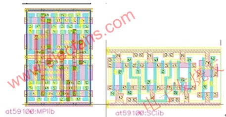
There is a new ASIC technology that uses a metal-programmable cell structure (MPCF) to achieve silicon efficiency comparable to that of cell ASICs (170K-210K gates/mm2 on 130nm process). For example, at 130nm process node, the silicon area used to implement a D flip-flop (DFF) using MCPF is almost the same as that of a standard cell (Figure 1: D flip-flop implemented with 130nm MPCF and 130nm standard cell).
MPCF technology is currently being used to develop customizable microcontrollers that not only have the ultra-low single-chip cost advantage of unit ASICs, but also have the advantages of low NRE and less than two months of design turnaround of structured ASICs. Basically, existing MCUs with SoC-level integration combined with metallized programmable cell structures can be used to implement customizable SoC platforms.
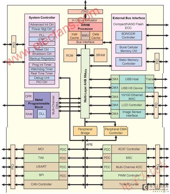
As an example of such a customizable microprocessor, it takes an existing MCU based on the 200 MHz ARM926EJ-S, with tightly coupled program and data caches of 16 Kbytes each for deterministic processing, 32 Kbytes of additional SRAM, 32 Kbytes of ROM, and peripherals to support networking, data transfer, and human machine interfaces, and adds a metallized programmable block (MP) equivalent to 28K or 56K FPGA LUTs (250K or 500K routable ASIC gates). (Figure 2 - AT91CAP9 block diagram). Peripherals already on the device include USB host and device, 10/100 Ethernet MAC, LCD controller, and image sensor interfaces for connecting to CAN, MCI, and SPI buses.

Figure 1: D flip-flop implemented using 130nm MPCF and 130nm standard cells.

Figure 2: AT91CAP9 block diagram.
The MP block implemented with MPCF technology is large enough to implement a secondary ARM processor core, a digital signal processing (DSP), some additional standard (or non-standard) interfaces, and other complex logic blocks, such as a GPS ring demodulator. It has many inherent functions and dedicated external connections to improve the efficiency of implementing special application logic units. It contains multiple distributed single-port and dual-port RAM blocks, which can be tightly coupled with the logic units that need them. The clock of the MP block can come from all clocks of the clock generator and the power management controller. This provides maximum flexibility for the timing of the special application logic units implemented inside it.
All peripherals implement DMA for data transfer between peripherals and memory. Otherwise, data transfer between peripherals and memory would exhaust the ARM9's resources. For example, a high-speed SPI data transfer at 20Mbps would require all the ARM cycles. Simple DMA is implemented on chip for each peripheral and managed by a DMA controller that offloads the data transfer task, so that 88% of the ARM9 cycles can be used for program processing while performing 20Mbps SPI transfers (Figure 2). In addition, there is a four-channel DMA controller responsible for the Ethernet MAC, LCD controller, and camera interface.
A six-layer Advanced High-Speed Bus (AHB) matrix with six masters and six slaves completely eliminates bus contention. The six masters are CPU data, CPU instruction, peripheral DMA controller, Ethernet, and USB host. The six slaves are memory, USB devices, and peripheral bus bridges. Any master can take control of any available bus when needed. Because there are as many buses as masters, there is no bus contention at all.
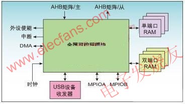
The external connections of the MP block include multiple master and slave connections to the AHB bus matrix, a set of interrupt lines for peripherals implemented in the MP block, a set of peripheral enable lines, two sets of parallel dedicated I/O ports, and a multiplexed connection to the USB receiver. In this way, a second USB device can be implemented in the MP block.
The chip includes an SD/MMC memory card interface (MCI) and an external bus interface (EBI) that support SDRAM, NAND Flash with error correction (ECC) and CompactFlash that can be connected to the on-board GByte-plus True IDE mode interface or removable storage including USB memory sticks.
A fully integrated system controller supports real-time operation by managing interrupt handling, reset, startup/shutdown, timing, power management, and parallel I/O control of the device.
Metal programmable blocks
The metal programmable block has numerous internal functions and specialized external connections to improve the efficiency of implementing application-specific logic units. Internally, it contains multiple single-ended/dual-port RAM blocks that are tightly coupled to the logic units that need them (Figure 3: Metal Programmable Block Interface).

Figure 3: Metal programmable block interface.
MP's external connections include:
1. Multiple parallel master and slave connections connected to the AHB bus matrix. Together with dedicated DMA channels, they can be configured to generate high-bandwidth data links connected to special application logic units. If APB peripherals are required in the MP block, an AHB/APB bridge and peripheral DMA controller (PDC) can be built internally to provide the required interface;
2. A set of interrupt lines. The interrupt lines enable the special application logic unit to generate interrupts handled by the advanced interrupt controller;
3. A set of peripheral enable lines. It allows the application-specific logic unit to connect or disconnect peripherals in the fixed ports of the device;
4. Two sets of parallel dedicated I/O ports. They provide a large number of external I/Os for special application logic units, and also provide electrical characteristics of I/Os connected to MP blocks;
5. A multiplexed connection to the USB receiver. This allows a second USB device to be implemented in the MP block.
The MP block can be clocked by all clocks from the clock generator and the power management controller. This provides maximum flexibility in the timing of the application-specific logic cells implemented inside it.
Design Process
The design process for a customizable microcontroller based on MPCF is very similar to the design process using an off-the-shelf ARM9 MCU and FPGA. In fact, the MCU+FPGA design may be mass-produced to test the market. Once proven successful, the entire design process can be directly ported to the customizable microcontroller.
The FPGA register transfer level (RTL) netlist can be directly ported to the MP functional block that already contains the AHB interface, DMA channels, and I/O channels.
Device drivers are provided for all peripherals/interfaces in the platform. They can also be used as templates for equivalent drivers for peripherals/interfaces defined in MP function blocks.
Industry-leading operating systems have been ported to customizable microprocessor architectures. Integration of these software modules with application code modules and user interfaces can be done in parallel with hardware development.
System specifications and hardware/software partitioning
A major advantage of the customizable MCU design flow is that the hardware/software can be verified and corrected if necessary during the simulation phase before hardware production. This saves time and expensive respins.
The work of customizing MP function blocks is usually completed by the customer and a qualified third-party design company. The first stage is mainly to develop the hardware block and related software drivers for the special application. In most cases, the hardware block is coded in Verilog RTL, while the software development is in C, C++ or ARM assembly language.
Placeholder instantiations of function blocks that have been written into templates provided by the MCU vendor and developed for the MP Block RTL code can simplify the integration of application-specific function blocks into the MP function blocks. Different templates are provided for AHB master/slave devices and APB slave devices. In some function blocks, DMA or PDC connections are pre-programmed. For example, the HDL for an APB connection function with a PDC connection is as follows:
The compatibility between the RTL code of the MP functional block and the fixed port of the microcontroller needs to be verified. The RTL code is then synthesized using the process-specific target library provided by the vendor and a functional simulation is performed on the entire device.
The low-level device drivers for the platform are provided by the MCU manufacturer, while the drivers for the MP function blocks come from the user or a third-party design company. These drivers are then integrated with the application modules that program the MCU and peripherals/interfaces. If an operating system is required, a pre-ported version can be obtained from a qualified third party and integrated into the software package. The software package also needs to be tested using industry-standard development tools. Of course, hardware/software co-simulation can also be performed at this stage.
simulation
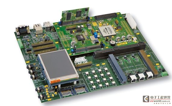
The key step in the design process is the simulation of the hardware and at least the low-level software. The AT91CAP simulation board includes a fully complementary memory, standard interfaces, networks and configurable connections (Figure 4: AT91CAP simulation board).

Figure 4: AT91CAP emulation board.
Practical experience has shown that this simulation step almost always finds various errors in the device's hardware and/or software, or in the device's hardware/software interface. The ability to correct and retest the complete device design at this stage is a major factor in reducing design time and design costs, which can increase the probability of first-time tape-out and software development success. An additional benefit is that the simulated version of the final design can be used as a starting point for future design iterations, thereby greatly saving design work.
Customizable MCU vendors perform placement and routing using a floor plan established for fixed ports of devices and MP blocks. Only the metal layers of the MP blocks need to be placed and routed. Post-layout simulation ensures that timing constraints are not violated.
One of the advantages of this solution is that the design team can complete software development without waiting for the design prototype. The development and testing of application software can be carried out simultaneously with layout and wiring and prototype manufacturing. Once the device and software are verified in the target application, the customer can formally approve the mass production of the product based on the rolling forecast. Because the inventory of blank wafers is in hand, the actual output can be adjusted at any time according to market demand.
When device volume requirements justify the investment, the netlist can be remapped to a fully standard cell design, bringing the advantages of reduced die size, improved performance, and lower power consumption.
ASIC price/performance without ASIC NRE and design cycle
Customizable microcontrollers with metal programmable cell structures can help designers integrate their custom IP into quasi-off-the-shelf solutions. It can provide the cost, power and performance advantages of full-custom ASICs, while the NRE and design cycle are not much different from off-the-shelf MCU+FPGA designs.
Previous article:Hardware Design of Radio Station Detection Controller Based on ARM Processor
Next article:Application of ARM9 in Temperature Control System of High Precision Biochemical Analyzer
Recommended ReadingLatest update time:2024-11-17 05:34


- Popular Resources
- Popular amplifiers
-
 Analysis and Implementation of MAC Protocol for Wireless Sensor Networks (by Yang Zhijun, Xie Xianjie, and Ding Hongwei)
 -
 MATLAB and FPGA implementation of wireless communication
 -
 Intelligent computing systems (Chen Yunji, Li Ling, Li Wei, Guo Qi, Du Zidong)
 -
 Summary of non-synthesizable statements in FPGA
 Professor at Beihang University, dedicated to promoting microcontrollers and embedded systems for over 20 years.
- Innolux's intelligent steer-by-wire solution makes cars smarter and safer
- 8051 MCU - Parity Check
- How to efficiently balance the sensitivity of tactile sensing interfaces
- What should I do if the servo motor shakes? What causes the servo motor to shake quickly?
- 【Brushless Motor】Analysis of three-phase BLDC motor and sharing of two popular development boards
- Midea Industrial Technology's subsidiaries Clou Electronics and Hekang New Energy jointly appeared at the Munich Battery Energy Storage Exhibition and Solar Energy Exhibition
- Guoxin Sichen | Application of ferroelectric memory PB85RS2MC in power battery management, with a capacity of 2M
- Analysis of common faults of frequency converter
- In a head-on competition with Qualcomm, what kind of cockpit products has Intel come up with?
- Dalian Rongke's all-vanadium liquid flow battery energy storage equipment industrialization project has entered the sprint stage before production
- Allegro MicroSystems Introduces Advanced Magnetic and Inductive Position Sensing Solutions at Electronica 2024
- Car key in the left hand, liveness detection radar in the right hand, UWB is imperative for cars!
- After a decade of rapid development, domestic CIS has entered the market
- Aegis Dagger Battery + Thor EM-i Super Hybrid, Geely New Energy has thrown out two "king bombs"
- A brief discussion on functional safety - fault, error, and failure
- In the smart car 2.0 cycle, these core industry chains are facing major opportunities!
- Rambus Launches Industry's First HBM 4 Controller IP: What Are the Technical Details Behind It?
- The United States and Japan are developing new batteries. CATL faces challenges? How should China's new energy battery industry respond?
- Murata launches high-precision 6-axis inertial sensor for automobiles
- Ford patents pre-charge alarm to help save costs and respond to emergencies
- The pain of vias, isn’t it just a window opened in the via, how can it cause a short circuit?
- About TAS5805M Stereo Class-D Amplifier
- 【GD32L233C-START Review】9. CRC Check
- Why is millimeter wave so important to 5G networks? How do 5G networks use millimeter wave?
- Share: How to use a microcontroller to control the output voltage of TPS5430?
- 5 Fill in the previous pit, TRACE32 download algorithm of GD32L233C,
- Problems with IC amplifiers
- Detailed explanation of terminal device state switching in TI ZigBee protocol stack
- NEC microcontroller
- [Flower carving DIY] Interesting and fun music visualization series of small projects (04) --- WS2812 strip light

 Analysis and Implementation of MAC Protocol for Wireless Sensor Networks (by Yang Zhijun, Xie Xianjie, and Ding Hongwei)


 京公网安备 11010802033920号