1. Introduction to 2440 clock
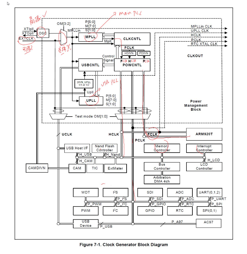
1.1 2440 is a SOC (system on chip) system, which not only has many CPUs, but also many peripherals. The system framework diagram in the 2440 chip manual is as follows:

In the 2440 framework diagram, there is not only a CPU, but also many peripherals, which are divided into two parts, one is the AHB bus and the other is the APB bus
1.2 AHB Bus
1.2.1 LCD Controller
1.2.2 USB Controller
1.2.3 NAND Controller
1.2.4 Memory Controller
1.2.5 Camera Interface
1.2.6 Interrupt Controller
1.2.7 Power management, etc.
1.3 APB Bus
1.3.1 UART
1.3.2 USB device
1.3.3 I2C
1.3.4 GPIO
1.3.5 RTC
1.3.6 ADC
1.3.7 Timers, etc.
1.4 Therefore, three clocks are introduced, FLCK, HCLK, PCLK
CPU works with FCLK, the maximum operating frequency is 400MHZ
AHB bus operates at HCLK, with a maximum operating frequency of 136MHZ
APB bus works with PCLK, the maximum operating frequency is 68MHZ
2. Obtaining the clock
2.1 The block diagram of the 2440 clock system is as follows

2.2 Clock Source Selection
As can be seen from the figure, there are two clock sources, namely external crystal oscillator and pin, which are selected by OM[3:2]. The mode selection is as shown in the figure below

In the schematic diagram of 2440, we can see that OM3 and OM2 are connected to GND, so we will choose to use an external crystal oscillator as the input.

2.3 Clock system flow
The 12MHZ crystal oscillator obtains FLCK through the MPLL phase-locked loop, and the CPU directly uses FCLK. FCLK is divided by PDIV to obtain PCLK for use by devices on the APB bus.
FCLK is divided by HDIV to obtain HCLK for use on the AHB bus
The 12MHZ crystal oscillator will also be provided to the USB through the UPLL phase-locked loop
3. Program Writing
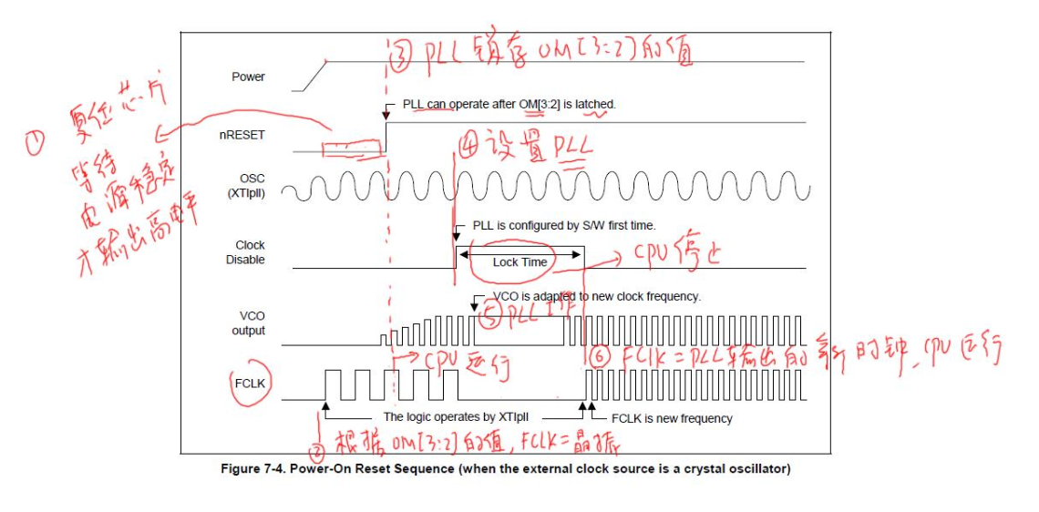
3.1 The timing diagram is as follows:

Note: Once the PLL is set, it will be locked for LOCK TIME until the PLL output is stable, and then the CPU starts working at the new frequency FCLK
3.2 Process Analysis
3.2.1 Once powered on, the reset pin will remain on for a while (waiting for the power supply to stabilize), and this is maintained by resetting the chip as follows:
3.2.2 According to the value of OM[3:2], FCLK is equal to 12M of the crystal oscillator.
3.2.3 PLL latches the value of OM[3:2] and the CPU starts running (the reset pin is pulled high)
3.2.4 Setting PLL
3.2.5 Setting the PLL after the CPU has stopped running for a period of time
3.2.6 After the setting is completed, FLCK is equal to the new frequency output by PLL
3.3 Register settings (target FCLK=400MZH, HCLK=100MZH, PCLK=50MHZ)
3.3.1 Set the LOCKTIME register to determine the LOCKTIME of MPLL and UPLL
Set to default value
3.3.2 Set the MPLLCON/UPLLCON register to determine FCLKi, as shown below

The formula is as follows:

The reference setting values are as follows. We select MDIV=92, PDIV = 1, SDIV=1 to set FCLK = 400MHZ:

MPLLCON = (92 << 12) | (1 << 4) | (1 << 0);
3.3.3 Setting the CLKCON register (turning off unused devices)
3.3.4 Set the CLKDIVN register to determine HCLK and PCLK, as shown below:

First, set bit[2:1] to 10. Then HCLK=FCLK/4=100MHZ, but CAMDIVN[9]=0 (the default value is 0) is required.
Set bit[0] to 1, then PCLK=HCLK/2=50MHZ
bit[3] takes the default value
3.3.5 If HDIVN is not equal to 0, the CPU must be set to asynchronous mode, and the CPU will work on HCLK, as shown below

For the assembly command orr r0,r0, #R1_nF:OR:R1_iA here, I consulted the relevant information and got a rough understanding: [It involves the C1 register of the coprocessor P15] You can refer to the following address to understand the coprocessor P15 (https://www.cnblogs.com/lifexy/p/7203786.html)
It turns out that the iA bit and nF bit control the CPU bus mode:
orr r0,r0,#R1_nF:OR:R1_iA
This command definitely means changing the CPU bus mode from "fast bus mode" to "asynchronous bus mode"
How to understand #R1_nF:OR:R1_iA? At first, I thought it was a command of the arm instruction. I found someone on the Internet who understood it as a conditional operator (exp1? exp2: exp3;). In fact, it is a pseudo code for setting the 30th and 31st positions of the R0 register to "1". So we will see the following code in the bootloader:
mrc p15,0,r0,c1,c0,0
orr r0,r0,#0xc0000000;R1_nF:OR:R1_iA
mcr p15,0,r0,c1,c0,0
So #R1_nF:OR:R1_iA means #0xc0000000
3.3.6 Increase the system clock code as follows (FCLK=400MHZ, HCLK=100MHZ, PCLK=50MHZ):
.text
.global _start
_start: /* 1. Turn off the watchdog */
ldr r0, =0x53000000
ldr r1, =0
str r1, [r0] /* 2. Set the clock*/
/* 2.1 Set LOCKTIME(0x4C000000)=0xFFFFFFFF */ ldr r0, =0x4C000000
ldr r1, =0xFFFFFFFF
str r1, [r0] /* 2.2 Set CLKDIVN(0x4C000014) = 0x5 FCLK : HCLK : PCLK = 400m : 100m : 50m*/ ldr r0, =0x4C000014
ldr r1, =0x5
str r1, [r0] /* 2.3 Set the CPU to asynchronous mode*/
mrc p15,0,r0,c1,c0,0
orr r0,r0,#0xc0000000 /* #R1_nF:OR:R1_iA */
mcr p15,0,r0,c1,c0,0 /* 2.4 Set MPLLCON(0x4C000004)=(92<<12) | (1 << 4) | (1 << 0)
* m = MDIV + 8 = 100
* p = PDIV + 2 = 3
* s = SDIV = 1
*Mpll = (2 * m * Fin) / (p * 2 ^ s) = (2 * 100 * 12) / (3 * 2 ^ 1) = 400MHZ
*/
ldr r0, =0x4C000004
ldr r1, =(92<<12) | (1 << 4) | (1 << 0)
str r1, [r0]
/* Once the PLL is set, the lock time will be locked until the PLL output is stable
* Then the CPU operates at the new frequency FCLK
*/
/* 3. Set up the stack
* Automatically distinguish NOR boot or NAND boot
* Write 0 to address 0, and read it out. If it is written, it is NAND, otherwise it is NOR
*/ ldr r0, =0
ldr r1, [r0] /* read out the original value backup*/
str r0, [r0] /* write 0 to address 0 */
ldr r2, [r0] /* read again*/
cmp r1, r2
ldr sp, =0x40000000 + 4096 /* nor start*/
moveq sp, #4096 /* nand start */
streq r1, [r0] /* restore the original value */ bl main
halt:
b halt
Previous article:S3C2440 I2C bus control
Next article:S3C2440 DMA driver example
Recommended ReadingLatest update time:2024-11-16 10:39


- Popular Resources
- Popular amplifiers
-
 Practical Development of Automotive FlexRay Bus System (Written by Wu Baoxin, Guo Yonghong, Cao Yi, Zhao Dongyang, etc.)
 -
 RT-Thread Kernel Implementation and Application Development Practical Guide: Based on STM32
 -
 Principles and Applications of Single Chip Microcomputers (Second Edition) (Wanlong)
 -
 Analog CMOS Integrated Circuit Design (2nd Edition)
 Professor at Beihang University, dedicated to promoting microcontrollers and embedded systems for over 20 years.
- Innolux's intelligent steer-by-wire solution makes cars smarter and safer
- 8051 MCU - Parity Check
- How to efficiently balance the sensitivity of tactile sensing interfaces
- What should I do if the servo motor shakes? What causes the servo motor to shake quickly?
- 【Brushless Motor】Analysis of three-phase BLDC motor and sharing of two popular development boards
- Midea Industrial Technology's subsidiaries Clou Electronics and Hekang New Energy jointly appeared at the Munich Battery Energy Storage Exhibition and Solar Energy Exhibition
- Guoxin Sichen | Application of ferroelectric memory PB85RS2MC in power battery management, with a capacity of 2M
- Analysis of common faults of frequency converter
- In a head-on competition with Qualcomm, what kind of cockpit products has Intel come up with?
- Dalian Rongke's all-vanadium liquid flow battery energy storage equipment industrialization project has entered the sprint stage before production
- Allegro MicroSystems Introduces Advanced Magnetic and Inductive Position Sensing Solutions at Electronica 2024
- Car key in the left hand, liveness detection radar in the right hand, UWB is imperative for cars!
- After a decade of rapid development, domestic CIS has entered the market
- Aegis Dagger Battery + Thor EM-i Super Hybrid, Geely New Energy has thrown out two "king bombs"
- A brief discussion on functional safety - fault, error, and failure
- In the smart car 2.0 cycle, these core industry chains are facing major opportunities!
- The United States and Japan are developing new batteries. CATL faces challenges? How should China's new energy battery industry respond?
- Murata launches high-precision 6-axis inertial sensor for automobiles
- Ford patents pre-charge alarm to help save costs and respond to emergencies
- New real-time microcontroller system from Texas Instruments enables smarter processing in automotive and industrial applications
- Analysis of the working principles of seven triode collector DC circuits 5
- RS-232 to RS-485 converter for industrial long distance communication
- About the Wireless Charging Electric Car for the Undergraduate Group of the 2018 College Electronics Competition
- Are electronic engineers' desks always messy? Let's talk about it
- Telecom FPGA Design Experience.pdf
- Share Altium_Designer_Beta_19.1.5
- Confusion: Issues with LDO and LC filtering
- AD Design Tips
- [ESP32-S2-Kaluga-1 Review] 5. Use LGVL to create a low-level interface?
- Kill TPS54340


 Practical Development of Automotive FlexRay Bus System (Written by Wu Baoxin, Guo Yonghong, Cao Yi, Zhao Dongyang, etc.)


 京公网安备 11010802033920号